Semiconductor manufacture equipment control system and method

A control system and semiconductor technology, applied in the field of communications, can solve the problems of uncontrollable process reaction modules, inability to understand status information deeply, affecting production efficiency, etc., to simplify the overall control process, avoid information-based islands, and reduce efficiency. wasteful effect

Active Publication Date: 2006-10-25
BEIJING NAURA MICROELECTRONICS EQUIP CO LTD
View PDF0 Cites 4 Cited by
  • Summary
  • Abstract
  • Description
  • Claims
  • Application Information

AI Technical Summary

Problems solved by technology

This process requires multiple information interactions and verification processes between the factory system and equipment. The semiconductor processing process becomes more and more complex, and the material transfer becomes more and more frequent, which will greatly affect the efficiency of production.
[0007] Secondly, from the perspective of the factory's manufacturing process management, the factory's manufacturing execution system is only responsible for issuing process tasks to each device, and the specific task identification and execution are completed by the overall machine control module in coordination with the transmission and process response modules under its jurisdiction. The manufacturing execution system of the factory cannot control the process reaction module of each equipment, and cannot deeply understand the status of the machine, especially the status information of the process reaction module
As a result, it is impossible to coordinate manufacturing resources uniformly within the entire factory
[0008] Finally, from the perspective of factory automation, according to such an equipment control system, several major components of the factory automation system: material management system, manufacturing execution system and advanced process control system cannot be integrated
The above-mentioned three major systems are separate. Although the SEMI standard has formulated corresponding interface standards in the three fields, the "information island" in the factory formed by such separate systems will definitely hinder the improvement of the production efficiency of the semiconductor manufacturing factory.
On the other hand, semiconductor equipment manufacturers must also customize corresponding software / hardware for the three major systems, which increases the complexity and maintenance difficulty of semiconductor equipment

Method used


Image

  • Semiconductor manufacture equipment control system and method
  • Semiconductor manufacture equipment control system and method

Examples


Embodiment Construction

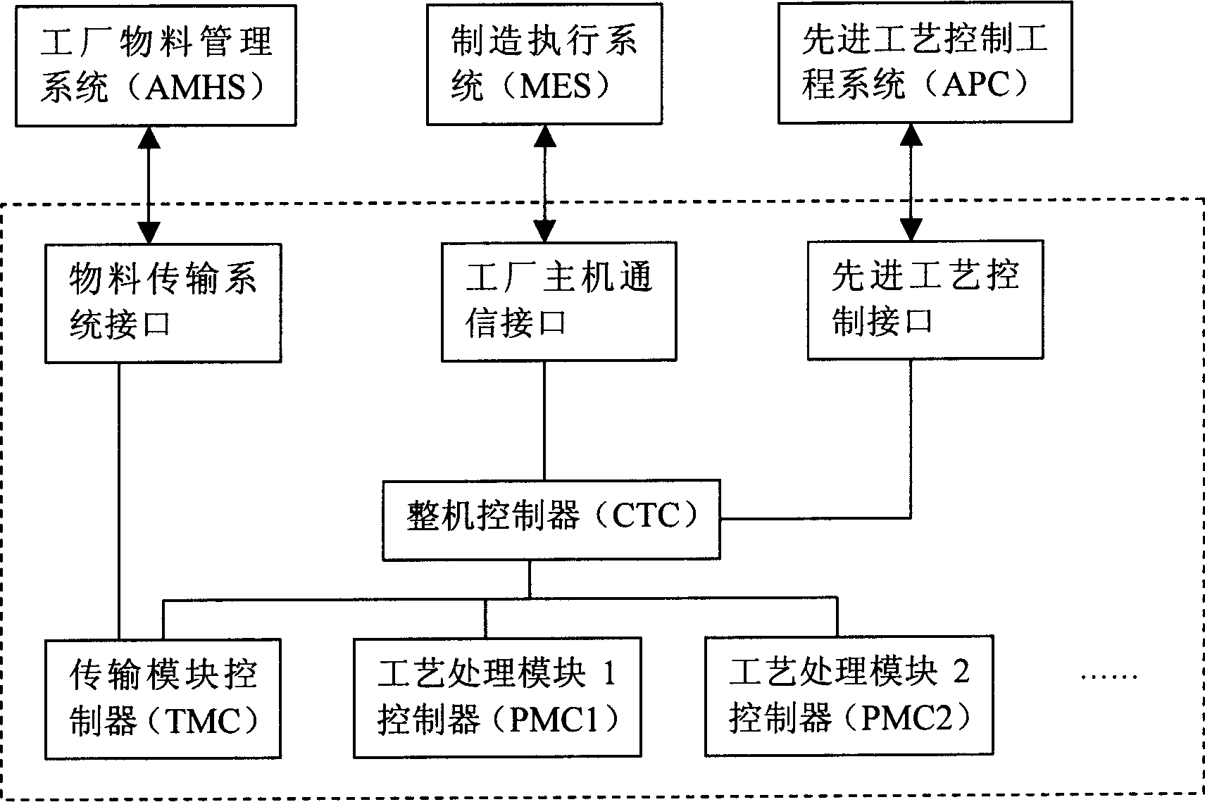
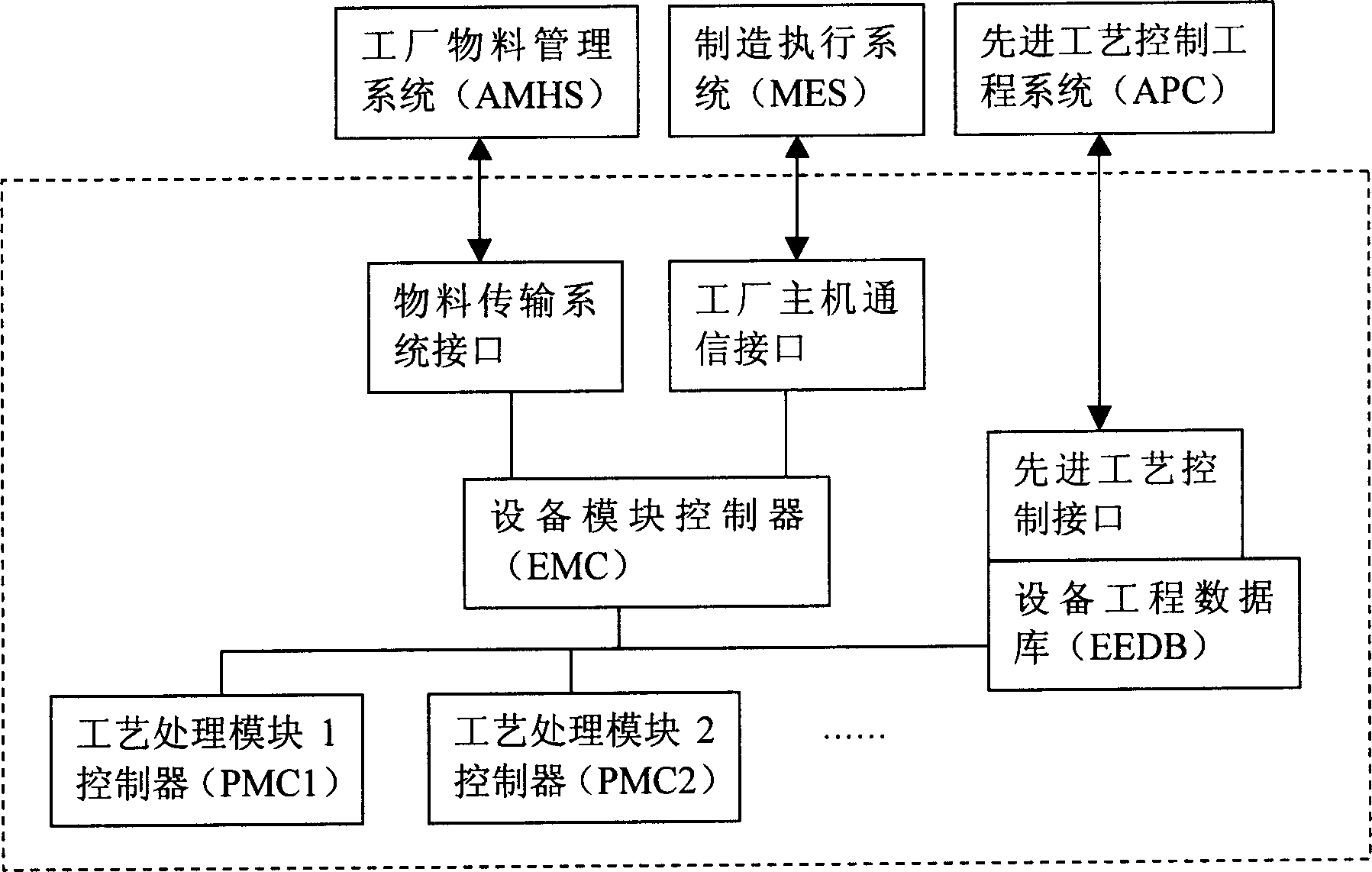
[0020] The following describes the communication method of the etching equipment subsystem of the present invention and the specific implementation of the device in further detail in conjunction with the accompanying drawings, but it is not used to limit the scope of protection of the present invention.

[0021] A semiconductor process equipment control system is composed of an equipment module controller (EMC), a process processing module controller (PMC), an equipment engineering database (EEDB), and corresponding interface modules. in:

[0022] As the unified controller of the factory, the equipment module controller (EMC) is responsible for the centralized management of the inflow and outflow of materials and the scheduling and transmission between different reaction modules of the equipment, and also executes the process processing tasks from the factory manufacturing execution system; at the same time, according to the preset The optimization algorithm and parameter valu...


PUM


Abstract

The present invention provides a semiconductor technology equipment control system, referring to communication field. Said control system consists of technology processing module controller (PMC) and relevant interface module, equipment module controller (EMC) and plant engineering data base (EEDB), wherein EMC used as integrating control unit connected with PMC, EEDB and interface module for total scheduling and controlling; EEDB connected with EMC and PMC for collecting and storing information from EMC and PMC and providing relevant parameter. The present invention can integrate three large systems at equipment terminal, greatly simplifying software and hardware configuring for semiconductor equipment manufacturer.

Description

technical field [0001] The invention relates to the communication field, in particular to a control system and a method thereof in semiconductor etching equipment. Background technique [0002] Modern large-scale integrated circuit manufacturing requires the use of dozens of process equipment for hundreds of processes. The equipment in an integrated circuit manufacturing plant is usually divided into several areas such as deposition, lithography, etching, and diffusion. Each The areas are all composed of semiconductor equipment processed by the same or similar process. The factory material transfer / management system (MHS) transfers materials between different regions, and the entire silicon wafer production process is coordinated by the factory-level Manufacturing Execution System (MES) to uniformly manage materials between different machines in different regions Coordination among them, and then complete the entire complex semiconductor process. With the continuous reduct...

Claims


Application Information

Patent Timeline
Patent Type & Authority Applications(China)
IPC IPC(8): G05B19/418G05B15/02H01L21/00
CPCY02P90/02
Inventor 史亚巍
Owner BEIJING NAURA MICROELECTRONICS EQUIP CO LTD
Why Eureka
Try Eureka