Metal oxide semiconductor field-effect transistor with isolating structure and its production

一种氧化物半导体、场效晶体管的技术,应用在金属氧化物半导体场效晶体管领域,能够解决制造过程复杂、高制作成本等问题,达到高击穿电压、低导通阻抗的效果

Active Publication Date: 2006-11-01
SYST GEN
View PDF0 Cites 2 Cited by
  • Summary
  • Abstract
  • Description
  • Claims
  • Application Information

AI Technical Summary

Problems solved by technology

However, the isolation structure formed by the above-mentioned traditional method not only has a complicated manufacturing process, but also requires a relatively high manufacturing cost.

Method used


Image

  • Metal oxide semiconductor field-effect transistor with isolating structure and its production
  • Metal oxide semiconductor field-effect transistor with isolating structure and its production
  • Metal oxide semiconductor field-effect transistor with isolating structure and its production

Examples


Embodiment Construction

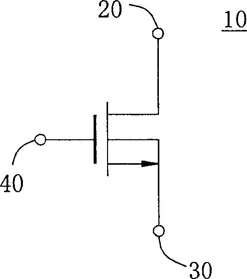
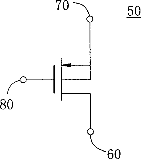
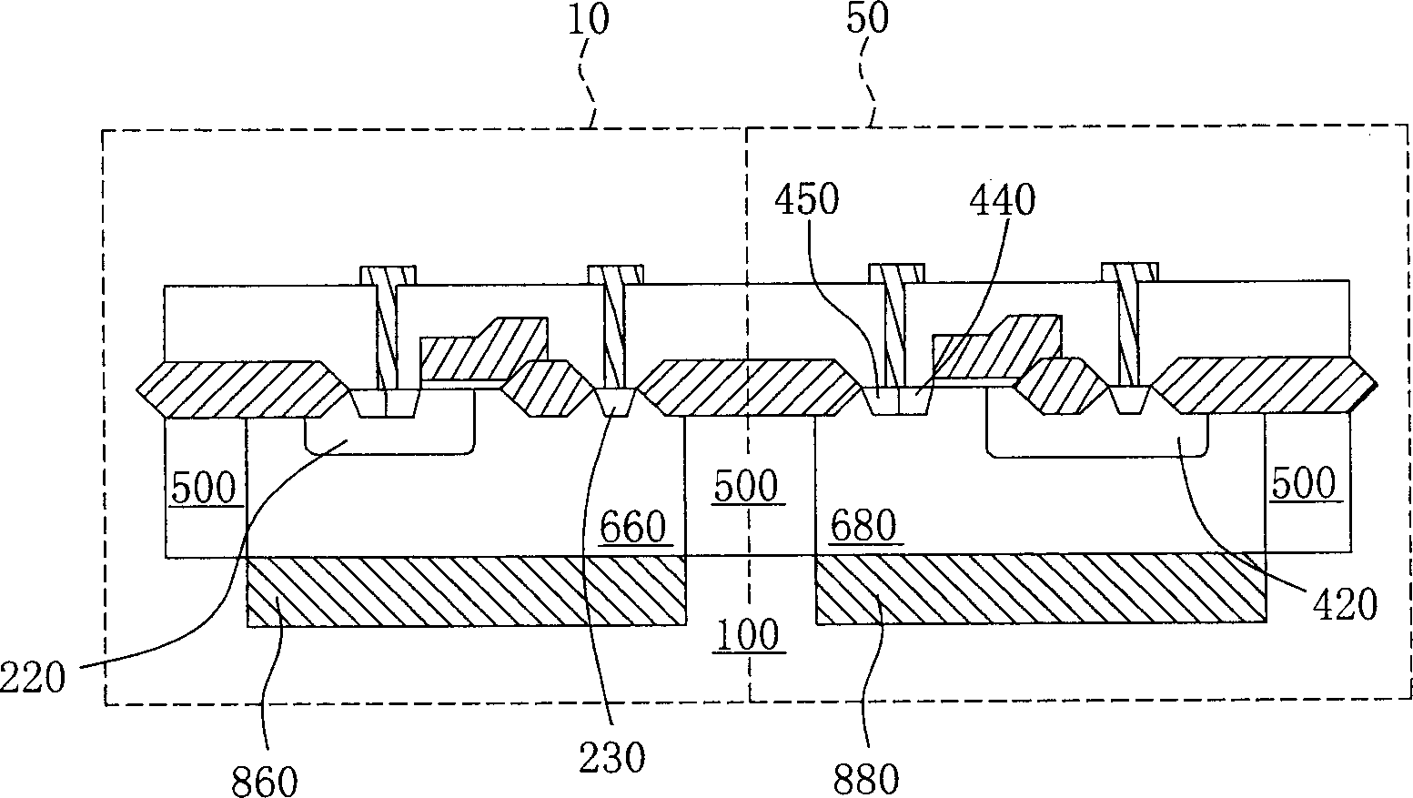
[0087] see Figure 4 and Figure 5 As shown, it is a schematic top view of the area and a schematic cross-sectional view of the structure of the metal oxide semiconductor field effect transistor of the present invention. As can be seen from the figure, the present invention provides an N-type metal oxide semiconductor field effect transistor 10, which at least includes: a P-type substrate 100, a first N-type embedded layer (buried layer) 101 and a P-type epitaxial layer (epitaxial layer) 90 is placed in the P-type substrate 100, a first N-type diffusion region 21 with N-type conductive ions forms a first N-type well 210 in the first N-type embedded layer 101, a first N-type well 210 with The first P-type diffusion region 22 of P-type conductive ions forms a first P-type region 220 in the first N-type well 210, and a first drain diffusion region 23 with N+ type conductive ions forms in the first N-type well 210. A first drain region 230 is formed in the diffusion region 21, a...


PUM


Abstract

Wherein a n-type metal oxide semiconductor field effect transistor (MOSFET) comprises a first n-type embedded layer and a p-type epitaxial layer, and a p-type MOSFET comprises a second embedded layer formed in the P-type substrate and a p-type epitaxial layer. Said first layer, second embedded layer and epitaxial layers provide isolation between said MOSfETs. Multi p-type isolation regions formed in said p-type epitaxial layer provide further isolation effect: a first gap is formed in a first thick field oxide layer and a first p-type region to improve anti breakdown voltage performance of n-type MOSFET; a second gap is formed between a second thick field oxide and a second n-type well to improve anti breakdown voltage of p-type MOSFET.

Description

technical field [0001] The present invention relates to a metal oxide semiconductor field effect transistor with an isolation structure and a manufacturing method thereof, in particular to a metal oxide semiconductor field effect transistor (Metal Oxide Semiconductor FieldEffect Transistor). Background technique [0002] The technology of integrating control circuits and driving transistors has become the development trend of current power integrated circuits (Power IC). Therefore, if transistor devices can be made using standard manufacturing processes, it seems to be a better solution for monolithic IC integration. However, the transistors produced by today's standard manufacturing process are non-isolated structures, and the non-isolated transistor current may flow in the substrate and interfere with the control circuit; in addition, the transistor current may also generate ground bounce. , and affect the control signal of the control circuit, so the non-isolated struct...

Claims


Application Information

Patent Timeline
Patent Type & Authority Applications(China)
IPC IPC(8): H01L29/78H01L21/336H01L21/76H01L21/8234H01L21/8238H01L27/092
CPCH01L21/823814H01L21/823878H01L21/823892H01L27/0921H01L27/0928H01L29/1083H01L29/42368H01L29/66659H01L29/66681H01L29/7816H01L29/7835
Inventor 黄志丰简铎欣林振宇杨大勇
Owner SYST GEN
Why Eureka
Try Eureka