

Nano line array in multiplayer structure, and preparation method
A nanowire array, multi-layer structure technology, applied in the fields of nanostructure manufacturing, nanotechnology, nanotechnology, etc., can solve the problem that oxide multilayer nanowires have not been publicly reported, and it is difficult to obtain sulfide multilayer nanowires and devices. Unfavorable production and other problems, to achieve the effect of low cost, orderly arrangement and high production efficiency
- Summary
- Abstract
- Description
- Claims
- Application Information
AI Technical Summary
Problems solved by technology
Method used
Image

Examples
Embodiment 1
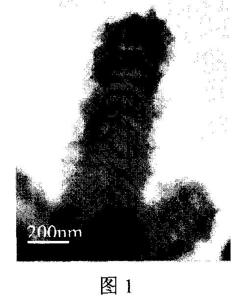
[0017] Example 1: Preparation of sulfide semiconductor / sulfide semiconductor nanowire arrays.
[0018] An aluminum oxide porous template coated with a 2 μm thick gold film on one side is selected, the pore diameter of the template is 100 nm, the hole spacing is 100 nm, and the thickness is 10 μm. The nickel / copper multilayer nanowire array is electrochemically deposited, and the nickel / copper plating electrolyte is composed of a mixed aqueous solution of copper sulfate (final concentration 0.2M) and nickel sulfate (final concentration 2M). Nickel (-1.4V) / copper (-0.3V) pulse alternating constant voltage growth method was used, and the deposition time was 1s and 10s, respectively. The thickness of the nickel / copper multilayer is 40nm / 20nm. The nanowire length is 1 μm. The template with nickel / copper multilayer nanowires grown in the hole is immersed in 3M NaOH solution to remove the aluminum oxide template, and a nickel / copper multilayer nanowire array regularly arranged on t...
Embodiment 2
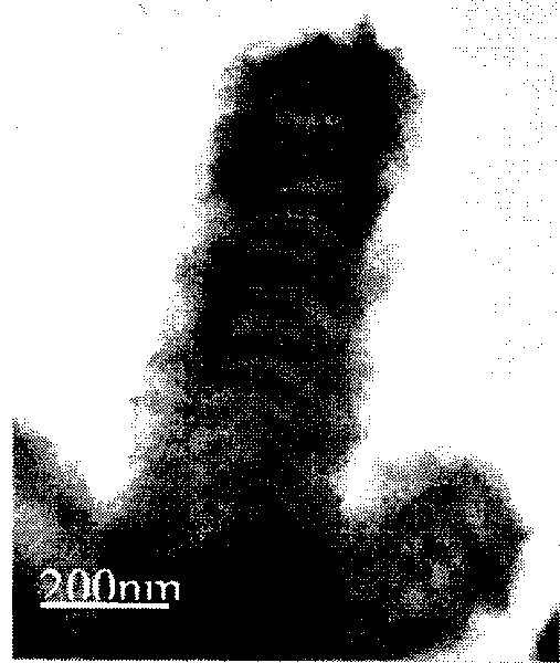
[0021] Embodiment 2: Preparation of an oxide semiconductor / oxide semiconductor nanowire array.
[0022] An aluminum oxide porous template coated with a 5 μm nickel film on one side is used to electrochemically deposit a nickel / copper multilayer nanowire array. The aperture of the template is 50 nm, the hole spacing is 100 nm, and the thickness is 10 μm. The nickel / copper plating electrolyte is composed of a mixed aqueous solution of copper sulfate (final concentration 0.2M) and nickel sulfate (final concentration 2M). The nickel (-1.4V) / copper (-0.3V) pulse alternating constant voltage growth method was adopted, and the deposition time was 1s and 10s, respectively. The thickness of the nickel / copper multilayer is 20nm / 40nm. The nanowire length is 1 μm.
[0023] The template with nickel / copper multilayer nanowires grown in the holes is immersed in 3M NaOH solution to remove the aluminum oxide template, and a nickel / copper multilayer nanowire array regularly arranged on the su...
Embodiment 3
[0026] Example 3: Preparation of metal sulfide semiconductor nanowire arrays.
[0027] A gold / iron multilayer nanowire array was electrochemically deposited on an aluminum oxide porous template coated with a 1 μm gold film on one side, with a template aperture of 80 nm, a hole spacing of 100 nm, and a thickness of 20 μm. Gold plating solution consists of HAuCl 4 ·3H 2 O(1gl -1 ) and H 2 SO 4 (7gl -1 ) composition, the iron plating solution consists of 0.5M FeSO4 and 0.5M H 2 SO4 solution composition. The process parameters of gold / iron multilayers were 10V, 2S and -1.5V, 3S, respectively, by double-groove alternating electrochemical constant-voltage deposition method. A gold / iron multilayer thickness of 20nm / 30nm was obtained. The nanowire length is 2 μm.
[0028] The template with gold / iron multilayer nanowires grown in the hole is immersed in 3M NaOH solution to remove the aluminum oxide template, and a gold / iron multilayer nanowire array regularly arranged on the s...
PUM
| Property | Measurement | Unit |
|---|---|---|
| thickness | aaaaa | aaaaa |
| diameter | aaaaa | aaaaa |
| length | aaaaa | aaaaa |
Abstract
Description
Claims
Application Information