Electronic device, semiconductor device and its manufacturing method

A manufacturing method and semiconductor technology, applied in semiconductor/solid-state device manufacturing, semiconductor devices, identification devices, etc., can solve problems such as high cost and achieve the effect of reducing cost

Inactive Publication Date: 2007-02-14
SEMICON ENERGY LAB CO LTD
View PDF0 Cites 13 Cited by
  • Summary
  • Abstract
  • Description
  • Claims
  • Application Information

AI Technical Summary

Problems solved by technology

However, this large-sized display requires high cost and a unique driving method due to the use of multiple panels

Method used


Image

  • Electronic device, semiconductor device and its manufacturing method
  • Electronic device, semiconductor device and its manufacturing method
  • Electronic device, semiconductor device and its manufacturing method

Examples


Embodiment 1

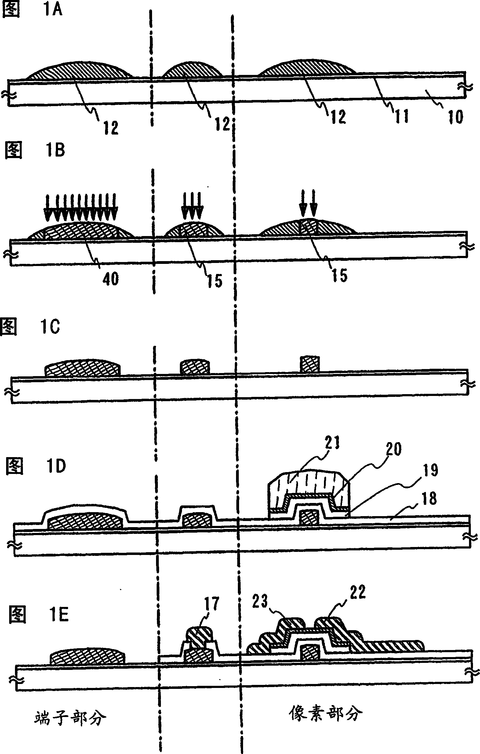
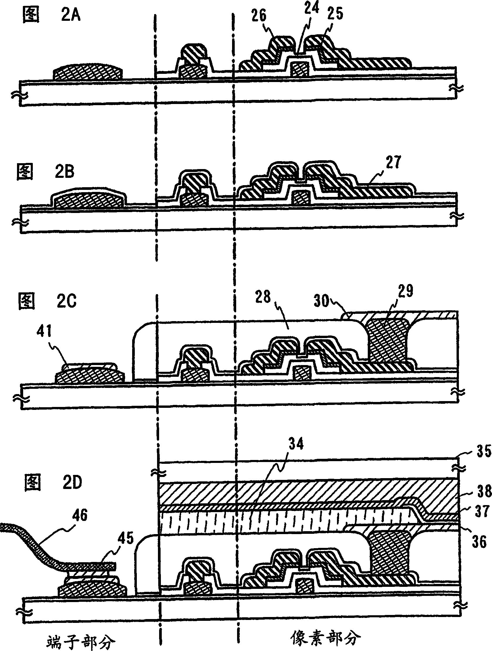
[0082] 1A to 2D show a method of manufacturing an active matrix light-emitting display device including a channel-etched TFT used as a switching element.

[0083] A base layer 11 for improving adhesion between the substrate 10 and a material layer subsequently formed by droplet discharge is formed on the substrate 10 . Since the base layer 11 is made to have an extremely thin thickness, it is not required that the base layer always have a layered structure. The preparation of the substrate layer 11 can be regarded as substrate pretreatment. Incorporation of photocatalyst materials (titanium oxide (TiO x ), strontium titanate (SrTiO 3 ), cadmium selenide (CdSe), potassium tantalate (KTaO 3 ), cadmium sulfide (CdS), zirconia (ZrO 2 ), niobium oxide (Nb 2 o 5 ), zinc oxide (ZnO), iron oxide (Fe 2 o 3 ), tungsten oxide (WO 3 )) Drops of treatment on the entire surface. Alternatively, selective formation of an organic material (polyimide, acrylic, or a coated insulating f...

Embodiment 2

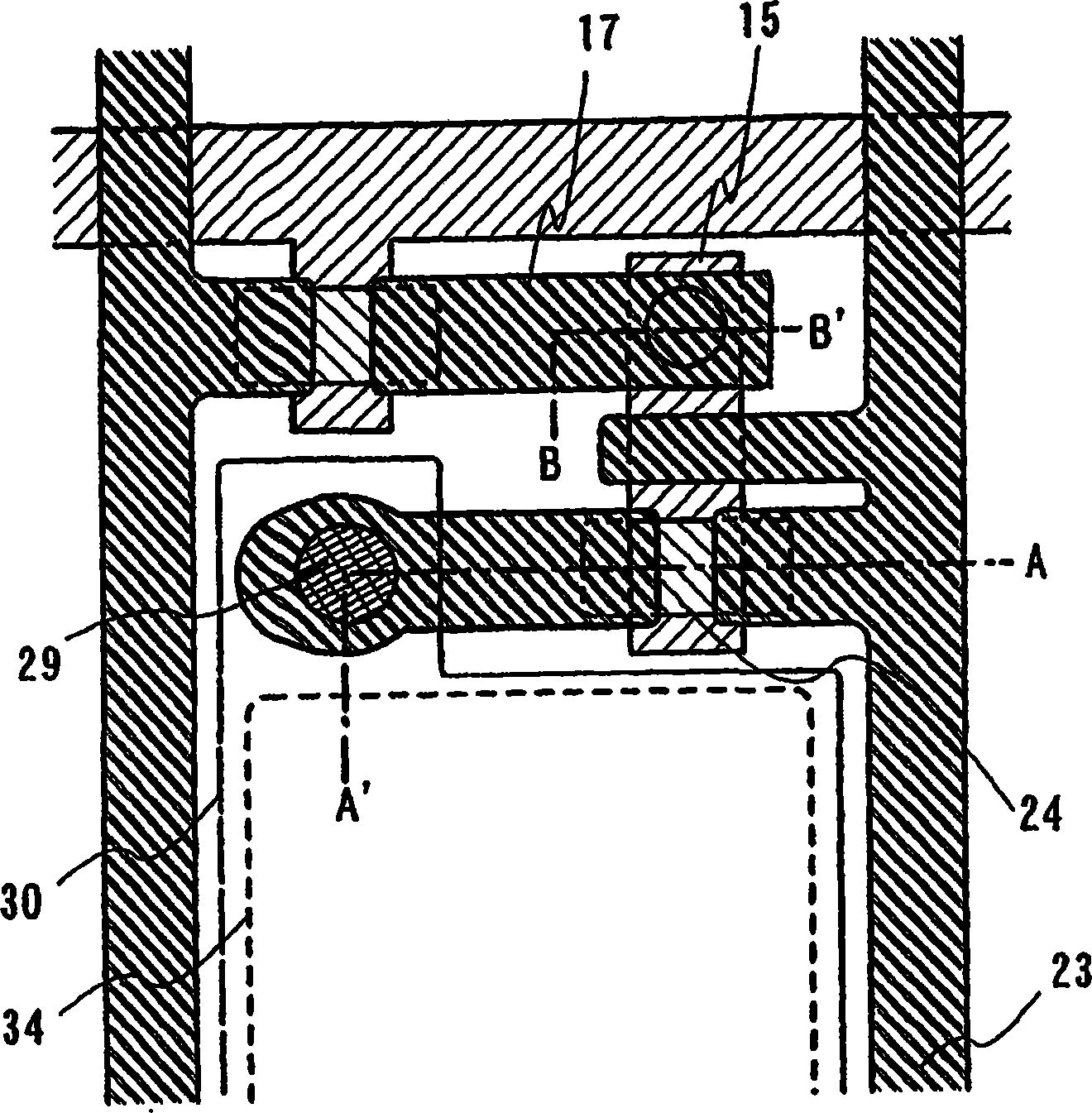
[0158] Embodiment 1 explains an example of exposing gate wiring by a laser beam drawing device. An example of a process of forming source wiring or gate wiring using a laser beam drawing device is described here with reference to FIG. 5 .

[0159] This process is slightly different from that shown in Example 1, so for the sake of simplicity, the same process part will not be further explained.

[0160] It is similar to Embodiment 1 until the patterning process of the semiconductor thin film is performed. Next, a conductive thin film pattern 220 is formed by droplet discharge (FIG. 5A). In the conductive film pattern 220, a positive type photosensitive material is mixed.

[0161] Next, use Figure 4 The apparatus shown selectively exposes the conductive film pattern 220 to laser light (FIG. 5B). The portion 221 irradiated by the laser undergoes a chemical reaction.

[0162] The portion 221 irradiated with laser light is removed by development, thereby forming source wiring...

Embodiment 3

[0168] 6A to 6D show examples of other processes. In FIGS. 6A to 6D , an example of using a planarizing film as the gate insulating film 260 is described. Other components are the same as those shown in Embodiment 2.

[0169] After forming the gate electrode, the gate insulating film 260 having a planar surface is formed by sputtering, planarizing a thin film obtained by chemical vapor deposition, or a coating method. This planarization treatment is typified by chemical mechanical polishing treatment.

[0170] When manufacturing a large-screen light-emitting display device, preferably, the gate wiring with low resistance is formed to have a large thickness, for example, 1 to 5 μm. When the cross-sectional area is increased by increasing the wiring thickness, a level difference between the substrate surface and the thick film wiring surface is generated, which leads to degradation of coverage. In the case of increasing the gate wiring thickness, the planar gate insulating fi...


PUM

PropertyMeasurementUnit
widthaaaaaaaaaa
tensile strengthaaaaaaaaaa
thicknessaaaaaaaaaa

Abstract

In the present circumstances, a film formation method of using spin coating in a manufacturing process is heavily used. As increasing the substrate size in future, the film formation method of using spin coating becomes at a disadvantage in mass production since a mechanism for rotating a large substrate becomes large, and there is many loss of material solution or waste liquid. According to the present invention, in a manufacturing process of a semiconductor device, a microscopic wiring pattern can be realized by delivering selectively photosensitive conductive material solution by droplet discharging, exposing selectively to laser light or the like, and developing. The present invention can reduce drastically costs since a patterning process can be shortened and an amount of material in a process of forming a conductive pattern can be reduced. Accordingly, the present invention can be applied to manufacture a large substrate.

Description

technical field [0001] The present invention relates to a semiconductor device having a circuit including a thin film transistor (hereinafter referred to as TFT) and a method of manufacturing the semiconductor device. More specifically, the present invention relates to an electric appliance equipped with an electro-optical device typified by a light-emitting display device having an organic light-emitting element or a liquid crystal display panel. [0002] The term "semiconductor device" as used herein refers to devices that can generally operate by utilizing semiconductor properties, such as electro-optical devices, semiconductor circuits, and electric appliances. Background technique [0003] In recent years, attention has been drawn to a technique of producing a thin film transistor (TFT) using a semiconductor thin film formed on a substrate having an insulating surface. Thin film transistors are widely used in electronic devices such as ICs or electro-optical devices, a...

Claims


Application Information

Patent Timeline
Patent Type & Authority Applications(China)
IPC IPC(8): G02F1/1368G02F1/1343G09F9/00H01L21/28H01L21/3205H01L21/336H01L29/417H01L29/423H01L29/49H01L29/786H05B33/14
Inventor 前川慎志山崎舜平小路博信
Owner SEMICON ENERGY LAB CO LTD
Why Eureka
Try Eureka