Nitride compound semiconductor device and process for producing the same

一种化合物系、制造方法的技术,应用在半导体/固态器件制造、半导体激光器、光波导半导体的结构等方向,能够解决难以实现激光振荡、结晶表面刮伤等问题,达到提高可靠性及制造成品率、降低电阻的效果

Inactive Publication Date: 2007-02-28
PANASONIC CORP
View PDF1 Cites 2 Cited by
  • Summary
  • Abstract
  • Description
  • Claims
  • Application Information

AI Technical Summary

Problems solved by technology

When GaN crystals are grown in this state on the main surface of such a GaN substrate, there is a problem that the crystal surface is largely affected by scratches.
[0016] According to the semiconductor laser disclosed in Patent Document 1, deterioration of crystallinity due to polycrystalline GaN precipitated on the mask layer can be suppressed. Also in the case of the structure formed by the method shown in FIG. 12, it is difficult to realize the required laser oscillation unless the voltage applied between the electrodes is increased.

Method used


Image

  • Nitride compound semiconductor device and process for producing the same
  • Nitride compound semiconductor device and process for producing the same
  • Nitride compound semiconductor device and process for producing the same

Examples


Embodiment approach 1

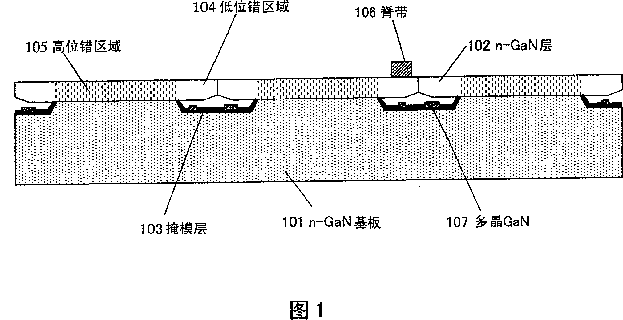
[0062] First, refer to FIG. 1 . FIG. 1 schematically shows a cross section of a nitride-based semiconductor device according to this embodiment.

[0063] The semiconductor device shown in FIG. 1 has a GaN substrate 101 with a plurality of band-shaped ridges formed on its main surface, and an n-GaN layer 102 grown on the GaN substrate 101 . In an actual semiconductor device, generally, a nitride-based semiconductor layer is also stacked on the n-GaN layer 102 . However, when the n-GaN layer 102 in FIG. 1 is used as a channel layer of a transistor or the like, a gate insulating film or a wiring structure is formed on the n-GaN layer 102 .

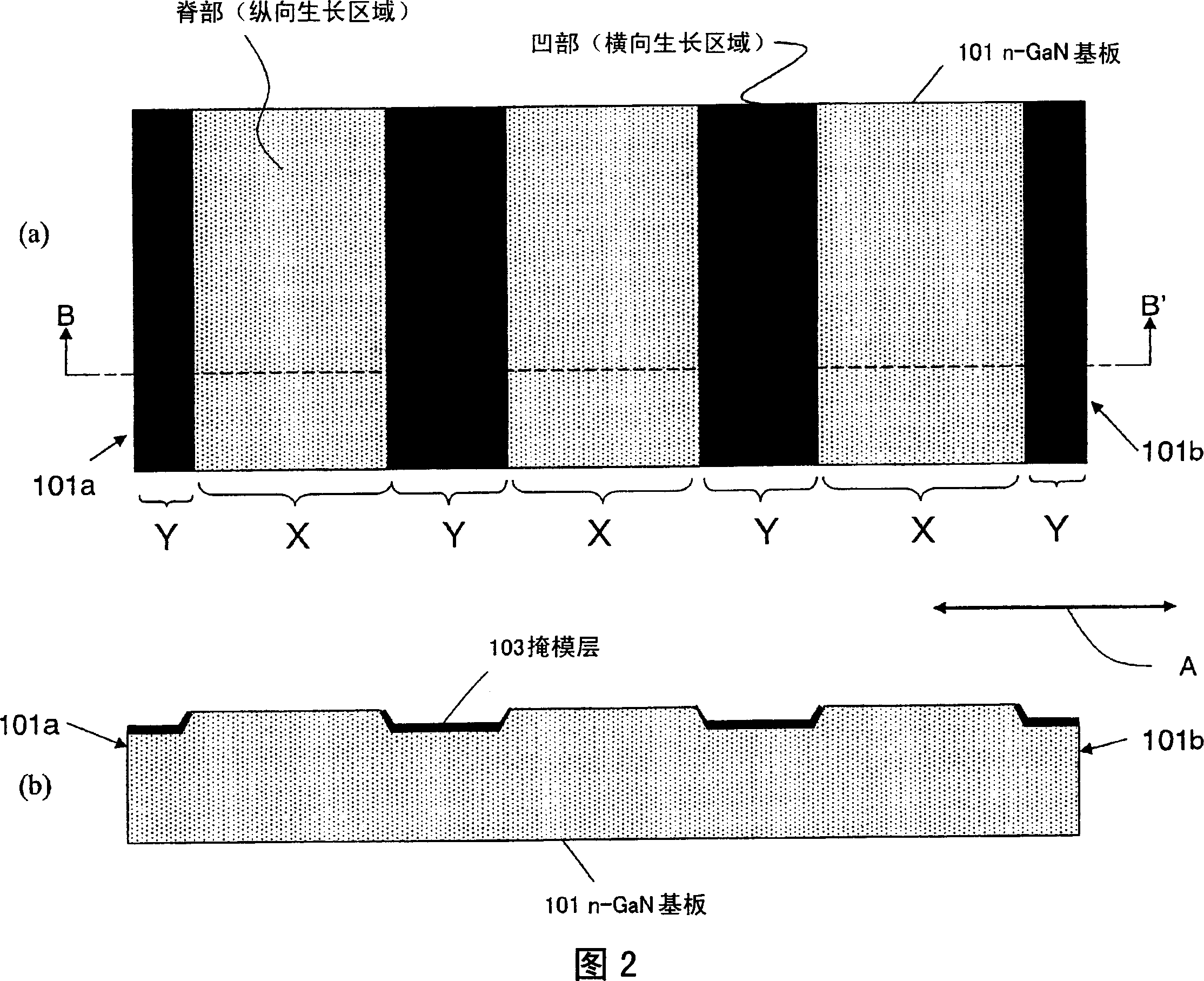
[0064] Referring to FIG. 2 , the structure of the GaN substrate 101 will be described in more detail. Fig. 2(a) is a plan view showing the principal surface of a GaN substrate 101 of a nitride-based semiconductor device, and Fig. 2(b) is a cross-sectional view along line B-B' thereof. As shown in FIG. 2 , the upper surface of the ridge por...

Embodiment approach 2

[0095] Next, a second embodiment of the nitride-based semiconductor device of the present invention will be described with reference to FIG. 6 . FIG. 6 schematically shows the cross-sectional structure of the nitrogen compound semiconductor laser of this embodiment.

[0096] The illustrated semiconductor laser includes an n-GaN substrate 101 in which a strip-shaped concave portion is formed on a main surface, and a semiconductor stacked structure grown on the GaN substrate 101 . The lowest layer of the semiconductor stack structure is the n-GaN layer 102 grown on the n-GaN substrate 10-. The n-GaN substrate 101 and n-GaN layer 102 of this embodiment are produced in the same manner as the n-GaN substrate 101 and n-GaN layer 102 of Embodiment 1 described above.

[0097] The above-mentioned semiconductor laminate structure is formed on the n-GaN layer 102 by forming an n-AlGaN type GaN superlattice contact layer 201, an n-AlGaN type GaN superlattice cladding layer 202, an n-GaN ...

Embodiment approach 3

[0106] Next, a third embodiment of the nitride-based semiconductor device of the present invention will be described with reference to FIG. 8 .

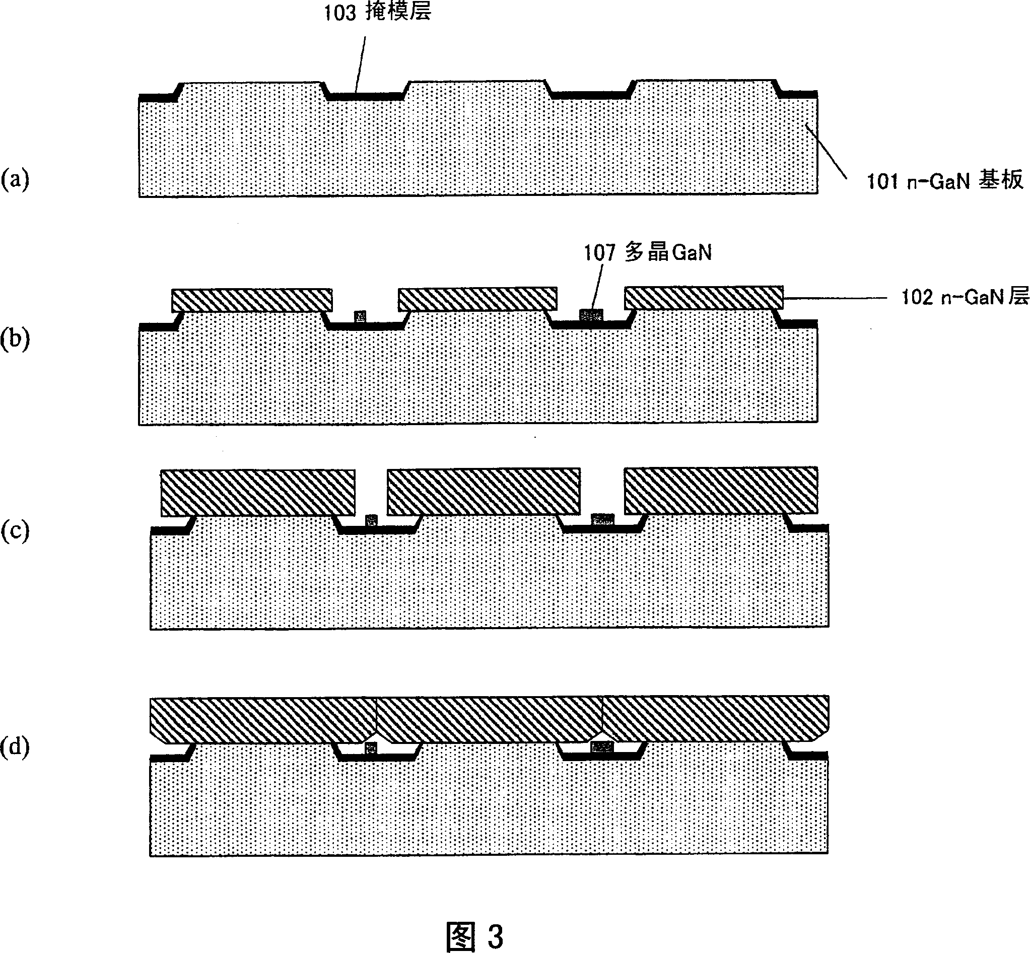
[0107] The structure of this embodiment differs from the structure shown in FIG. 1 in that a GaN layer 801 (thickness: 1 μm) is provided on the surface of the n-GaN substrate 101 of this embodiment. Specifically, after the GaN layer 801 is grown on the main surface of the n-GaN substrate 101, band-shaped ridges are formed on the main surface of the substrate by the method described in Embodiment Mode 1. FIG.

[0108] In this embodiment, the width X of the ridge (protrusion with resist) is set to about 20 μm, and the width Y of the concave portion is set to about 5 μm. The bottom and side surfaces of the recess are covered with a mask layer 103 made of SiO deposited by ECR sputtering or thermal CVD. 2 constitute.

[0109] The selective lateral growth of the n-GaN layer 102 is performed in the same manner as the method described in t...


PUM


Abstract

A nitride compound semiconductor device comprising conductive substrate structure (101) and, supported thereby, a semiconductor laminate structure. The major plane of the substrate structure (101) has not only at least one longitudinal growth region functioning as a seed crystal for longitudinal growth of nitride compound semiconductor but also multiple lateral growth regions realizing lateral growth of the nitride compound semiconductor having grown on the longitudinal growth region. When the total size of longitudinal growth region along the direction of arrow A is referred to as SX while the total size of multiple lateral growth regions along the same direction is referred to as SY, there is the relationship SX / SY>1.0.

Description

technical field [0001] The present invention relates to a nitrogen compound semiconductor device such as a semiconductor laser that can be used for optical information processing or display, and a method for manufacturing the same. Background technique [0002] The use of III-V nitride-based semiconductor materials headed by gallium nitride (GaN) (Al x Ga y In 1-x-y The blue-violet semiconductor laser produced by N(0≤x≤1, 0≤y≤1)) is a key device for ultra-high-density recording through optical disc devices, and has now reached a practical level. The higher output of blue-violet semiconductor lasers is not only a technology that enables high-speed writing of optical discs, but also a technology that is necessary for the development of new technology fields such as the application of laser displays. A conventional example of a blue-violet semiconductor laser is disclosed in Non-Patent Document 1, for example. [0003] In recent years, GaN substrates have attracted attentio...

Claims


Application Information

Patent Timeline
Patent Type & Authority Applications(China)
IPC IPC(8): H01S5/343H01S5/22H01L21/205
CPCH01L21/02639H01L21/02389H01S5/32341H01L21/0262H01L21/0265H01S2304/12H01S5/22H01L21/0254
Inventor 岛本敏孝川口靖利长谷川义晃石桥明彦木户口勋横川俊哉
Owner PANASONIC CORP
Why Eureka
Try Eureka