Semiconductor manufacturing process using ultra-low dielectric materials

A technology of ultra-low dielectric materials and low dielectric materials, which is applied in semiconductor/solid-state device manufacturing, circuits, electrical components, etc., can solve the problems of dielectric constant change, weak resistance to mechanical stress, and difficult to remove. To achieve the effect of preventing adverse effects

Inactive Publication Date: 2007-03-07
SHANGHAI INTEGRATED CIRCUIT RES & DEV CENT +1
View PDF0 Cites 3 Cited by
  • Summary
  • Abstract
  • Description
  • Claims
  • Application Information

AI Technical Summary

Problems solved by technology

[0012] However, the low dielectric constant material has a loose structure and soft hardness, and its ability to resist mechanical stress is very weak. This especially has a great impact on the chemical mechanical polishing process. The mechanical polishing process is indispensable. How to use the excellent performance of low dielectric materials and overcome its own shortcomings in chemical mechanical polishing has become the focus of the problem; secondly, due to the loose structure of low dielectric constant materials, in Plasma etching is easily damaged, and the organic polymer produced will be embedded in the loose structure, which is difficult to remove, so that the dielectric constant will change significantly, and the advantage of low dielectric constant will be lost. This is also the chip Producers do not want to see the results

Method used


Image

  • Semiconductor manufacturing process using ultra-low dielectric materials
  • Semiconductor manufacturing process using ultra-low dielectric materials
  • Semiconductor manufacturing process using ultra-low dielectric materials

Examples


Embodiment Construction

[0039] Now in conjunction with accompanying drawing, specific embodiment of the present invention is described in further detail:

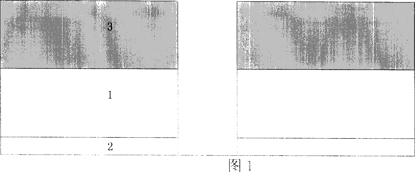
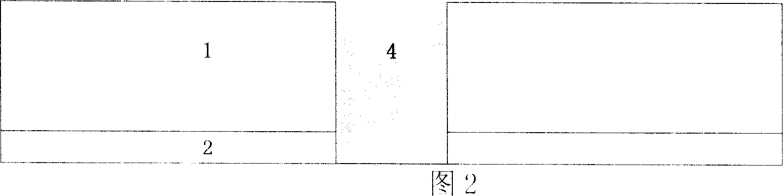
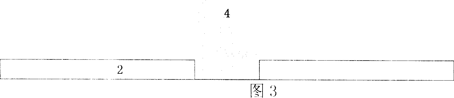
[0040]First, as shown in Fig. 1, the etching barrier layer 2 and the intermetallic dielectric layer 1 at the bottom of the growth metal wire, the etching barrier layer, its raw material source is helium, neon, argon, krypton or xenon inert gas, carbon monoxide, carbon dioxide, sulfur dioxide , silane, methane, or nitrogen, manufactured by process, the thickness is 30 nanometers, 40 nanometers, 50 nanometers, 60 nanometers, 70 nanometers. 80nm, 90nm, 100nm, 110nm, 120nm, each processing time is 50 seconds, 100 seconds, 150 seconds, 200 seconds, 250 seconds, 300 seconds, 350 seconds, 400 seconds, 450 seconds and 500 seconds , the air pressure is 5 Torr, 10 Torr, 30 Torr and 50 Torr, the power is 100 W, 150 W and 300 W respectively; the temperature is 150 ° C, 175 ° C, 200 ° C, 250 ° C, 300 ° C, 350 ° C At a temperature of 400°C, the product can be ...


PUM


Abstract

This invention discloses one semiconductor process method by use of super low medium materials which uses chemical agent reaction to remove metal medium materials after each layer of semiconductor metal process and fills low medium materials and then grow hard mask medium materials as protection layer on the low medium materials to process next layer of metal wire for repeating process to realize metal connection without chemical mechanic polishing damage.

Description

technical field [0001] The invention belongs to the technical field of integrated circuit technology, and in particular relates to a novel semiconductor manufacturing technology using ultra-low dielectric materials. Background technique [0002] With the continuous improvement of integrated circuit manufacturing technology, the volume of semiconductor devices is becoming smaller and smaller, and it is more difficult to connect them. In the past 30 years, the semiconductor industry has used aluminum as the material for connecting devices, but as chips shrink, the industry needs thinner and thinner connections, and the high resistance of aluminum is becoming more and more difficult to meet. need. And in the case of high-density VLSI, high resistance can easily cause electrons to "jump wires", causing nearby devices to generate false switching states. That is to say, chips with aluminum as wires may have unpredictable operation and poor stability. On such a tiny circuit, cop...

Claims


Application Information

Patent Timeline
Patent Type & Authority Applications(China)
IPC IPC(8): H01L21/768
Inventor 朱骏
Owner SHANGHAI INTEGRATED CIRCUIT RES & DEV CENT
Why Eureka
Try Eureka