
Production method of multilayer ceramic electronic device

A technology of electronic components and manufacturing methods, which is applied in the direction of capacitor manufacturing, laminated capacitors, fixed capacitor parts, etc., can solve the problems of deterioration of withstand voltage failure rate, thinning of dielectric layer, and short circuit failure rate, so as to prevent cracks, Improve the bonding strength and achieve the effect of electrostatic capacity

Active Publication Date: 2007-04-04
TDK CORPARATION
View PDF1 Cites 8 Cited by
  • Summary
  • Abstract
  • Description
  • Claims
  • Application Information

AI Technical Summary

Problems solved by technology

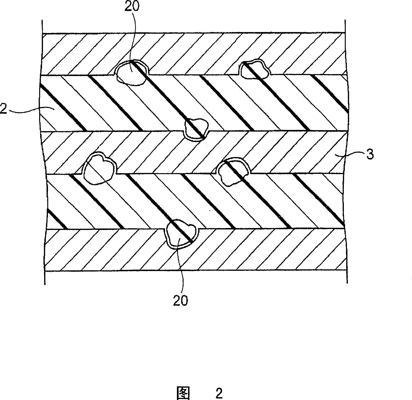
That is, when such a ceramic powder with a large particle size is used, the thickness of the adjacent dielectric layer is affected by the large particle size of the ceramic powder, and in particular, a phenomenon called a partial thinning of the adjacent dielectric layer occurs.
Furthermore, this is the reason, and as a result, there is also a problem that the short-circuit defect rate and withstand voltage defect rate deteriorate.

Method used

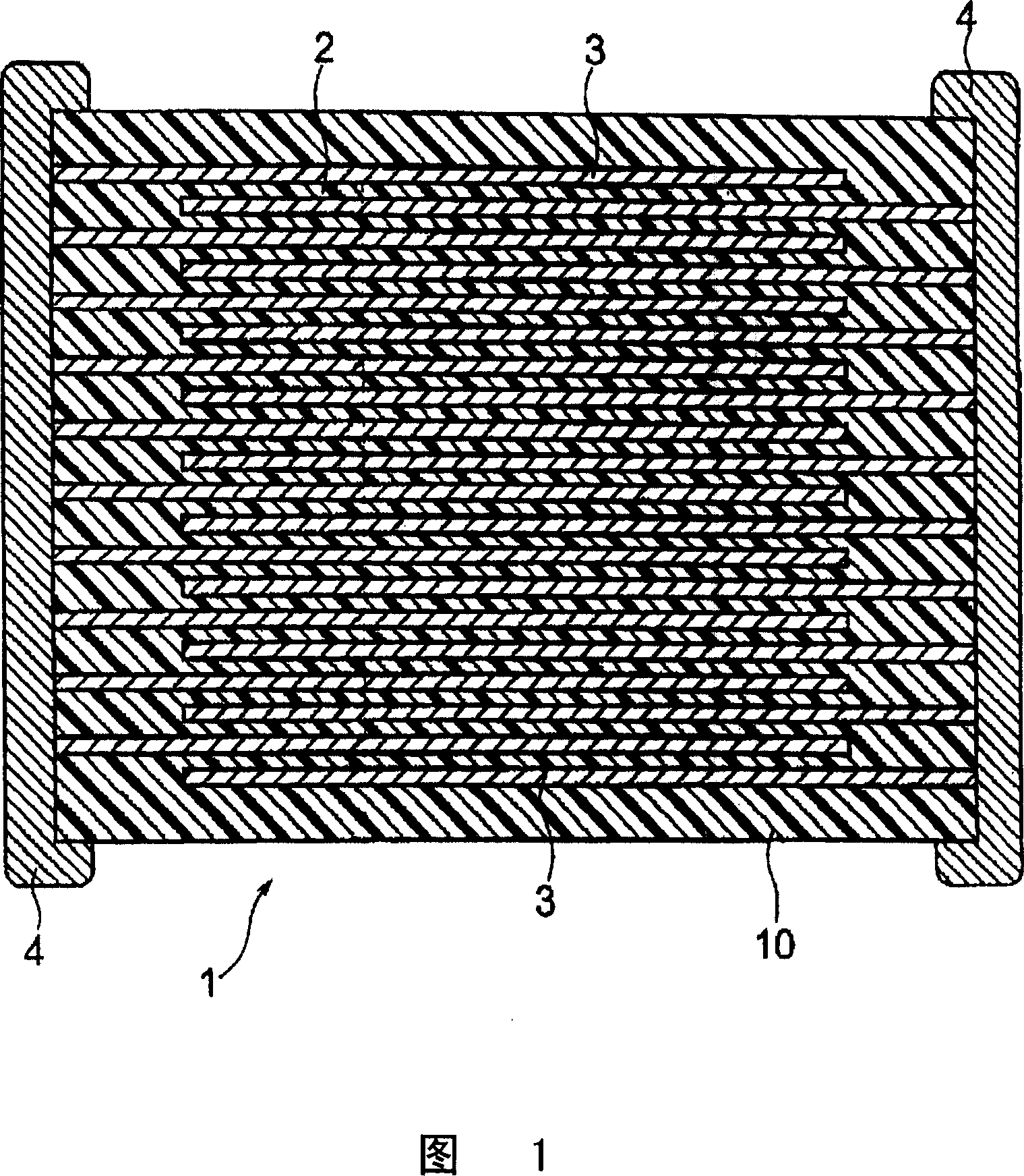
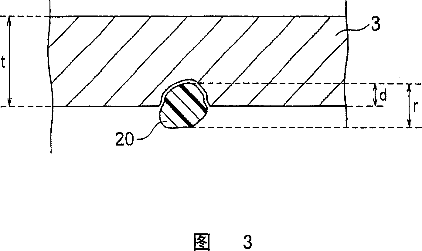

Image

  • Production method of multilayer ceramic electronic device
  • Production method of multilayer ceramic electronic device
  • Production method of multilayer ceramic electronic device

Examples


Embodiment 1

[0085] First, a main component material (BaTiO 3 ) and Y as a subcomponent raw material 2 o 3 , V 2 o 5 , CrO, MgO, SiO 2 and CaO. Next, the raw material prepared by wet mixing with a ball mill for 16 hours was prepared as a dielectric raw material.

[0086] Using a ball mill, mix the dielectric material prepared according to the above: 100 parts by weight, acrylic resin: 4.8 parts by weight, ethyl acetate: 100 parts by weight, mineral spirits: 6 parts by weight, toluene: 4 parts by weight, and make a paste to obtain Paste for dielectric layer.

[0087] Next, Ni particles with an average particle diameter of 0.2 μm: 100 parts by weight were kneaded by a 3-roll machine, and BaTiO as the first co-material 3 (average particle size: 0.05μm): 20 parts by weight, BaTiO as the second co-material 3 (average particle diameter: 0.5 μm): the amount shown in Table 1, organic vehicle (8 parts by weight of ethyl cellulose dissolved in 92 parts by weight of terpineol): 40 parts by we...

Embodiment 2

[0114] As the Ni powder contained in the conductor paste, while using Ni powder with an average particle diameter of 0.1 μm, and changing the content of the second co-material as shown in Table 2, a laminate was produced in the same manner as in Example 1. The ceramic capacitor samples were evaluated in the same manner as in Example 1. The results are shown in Table 2.

[0115] sample

[0116] From Table 2, when using Ni powder with an average particle diameter of 0.1 μm as the Ni powder, the same tendency as in Example 1 was confirmed.

Embodiment 3

[0118] Except changing the ratio of the first co-material contained in the conductive paste as shown in Table 3, a multilayer ceramic capacitor sample was produced in the same manner as in the sample No. 6 of Example 1, and evaluated in the same manner as in Example 1. The results are shown in Table 3.

[0119] sample

Numbering

conductor paste

Multilayer ceramic capacitor samples

Ni powder

(μm)

1st co-material

2nd common material

internal electrode

layer thickness

(μm)

2nd common material

particle size / internal

Electrode layer thickness

Crack incidence

(ppm)

Capacitance

(%)

short circuit

defective rate

(%)

withstand voltage

defective rate

(%)

(μm)

(parts by weight)

(μm)

(parts by weight)

Below 1000ppm

-10% or less

50% or less

50% or less

18

0.2

-

0

0.5

5

...


PUM

PropertyMeasurementUnit
particle sizeaaaaaaaaaa
thicknessaaaaaaaaaa
particle sizeaaaaaaaaaa

Abstract

A method of manufacturing a laminated ceramic electronic component having a dielectric layer and an internal electrode layer, wherein the conductive paste for forming the internal electrode layer contains at least a first common material composed of conductive particles and ceramic powder, and a ceramic A second co-material composed of powder and having an average particle diameter larger than the above-mentioned first co-material; the average particle diameter of the above-mentioned first co-material is 1 / 20 to 1 / 2 of the average particle diameter of the above-mentioned conductor particles Size, the average particle diameter of the above-mentioned second co-material is a size of 1 / 10 to 1 / 2 of the average thickness of the above-mentioned internal electrode layer after sintering A method for manufacturing a multilayer ceramic electronic component of a conductive paste, the present invention provides A method of manufacturing multilayer ceramic electronic components such as multilayer ceramic capacitors capable of effectively suppressing the occurrence of cracks, reducing short-circuit failure rates and withstand voltage failure rates, and having high electrostatic capacitance.

Description

technical field [0001] The present invention relates to a method for manufacturing multilayer ceramic electronic components such as multilayer ceramic capacitors, and more specifically, to a method capable of suppressing the occurrence of cracks, reducing short-circuit defect rates and withstand voltage defect rates, and having a high electrostatic capacitance. A method for manufacturing a multilayer ceramic electronic component. Background technique [0002] Multilayer ceramic capacitors, which are an example of multilayer ceramic electronic components, are widely used as small, large-capacity, and highly reliable electronic components, and the number of them used in a single electronic device is also greatly increasing. In recent years, along with the miniaturization and high performance of equipment, the requirements for the miniaturization, larger capacity, lower price, and higher reliability of multilayer ceramic capacitors have become more and more stringent. [0003]...

Claims


Application Information

Patent Timeline
Patent Type & Authority Applications(China)
IPC IPC(8): H01G4/30H01G4/12H01G13/00H01G4/232
CPCC04B2235/3418C04B2235/6584C04B2235/3236C04B2235/6588C04B2235/3241C04B2235/6567C04B2235/6565C04B2235/3225C04B2235/6562C04B35/4682C04B2235/5445C04B2235/3206H01G4/30C04B2235/3208C04B2235/6582H01G4/0085C04B35/638C04B2235/3239H01G4/12C04B2235/663
Inventor 小岛达也政冈雷太郎室泽贵子
Owner TDK CORPARATION
Learn More