Heterojunction bipolar transistor

A technology of bipolar transistors and heterostructures, applied in semiconductor devices, semiconductor/solid-state device manufacturing, electrical components, etc., can solve the problem of not reducing ΔEc well, deteriorating base layer and base/collector cross section Crystal quality, difficulty in obtaining satisfactory InAlAs/GaAsSb interface, etc.

Inactive Publication Date: 2007-05-16
NIPPON TELEGRAPH & TELEPHONE CORP
View PDF2 Cites 8 Cited by
  • Summary
  • Abstract
  • Description
  • Claims
  • Application Information

AI Technical Summary

Problems solved by technology

This limits the increase in As content and makes it impossible to reduce ΔEc well
Also, when layered structures are to be formed by metal-organic chemical vapor deposition (MOCVD), the aforementioned increase in tensile stress poses a new problem: the hydrogen passivation resistance of carbon acceptors in carbon-doped GaAsSb is greatly reduced. decrease
In addition to the problem of low n-type doping efficiency of the InAlAs layer, this material system also brings about the problem that the carriers are easily absorbed by the InAlAs doped with Si (usually used as n-type dopant). Fluorine (F) passivation
This increases the temperature difference from the growth temperature of the base layer (approximately 500°C under the same conditions), thereby deteriorating the crystal quality of the base layer and the base / collector section
In addition, it is difficult to obtain a satisfactory InAlAs / GaAsSb interface as described in Ref.

Method used


Image

  • Heterojunction bipolar transistor
  • Heterojunction bipolar transistor
  • Heterojunction bipolar transistor

Examples


Embodiment Construction

[0036] Embodiments of the present invention will be described below with reference to the drawings.

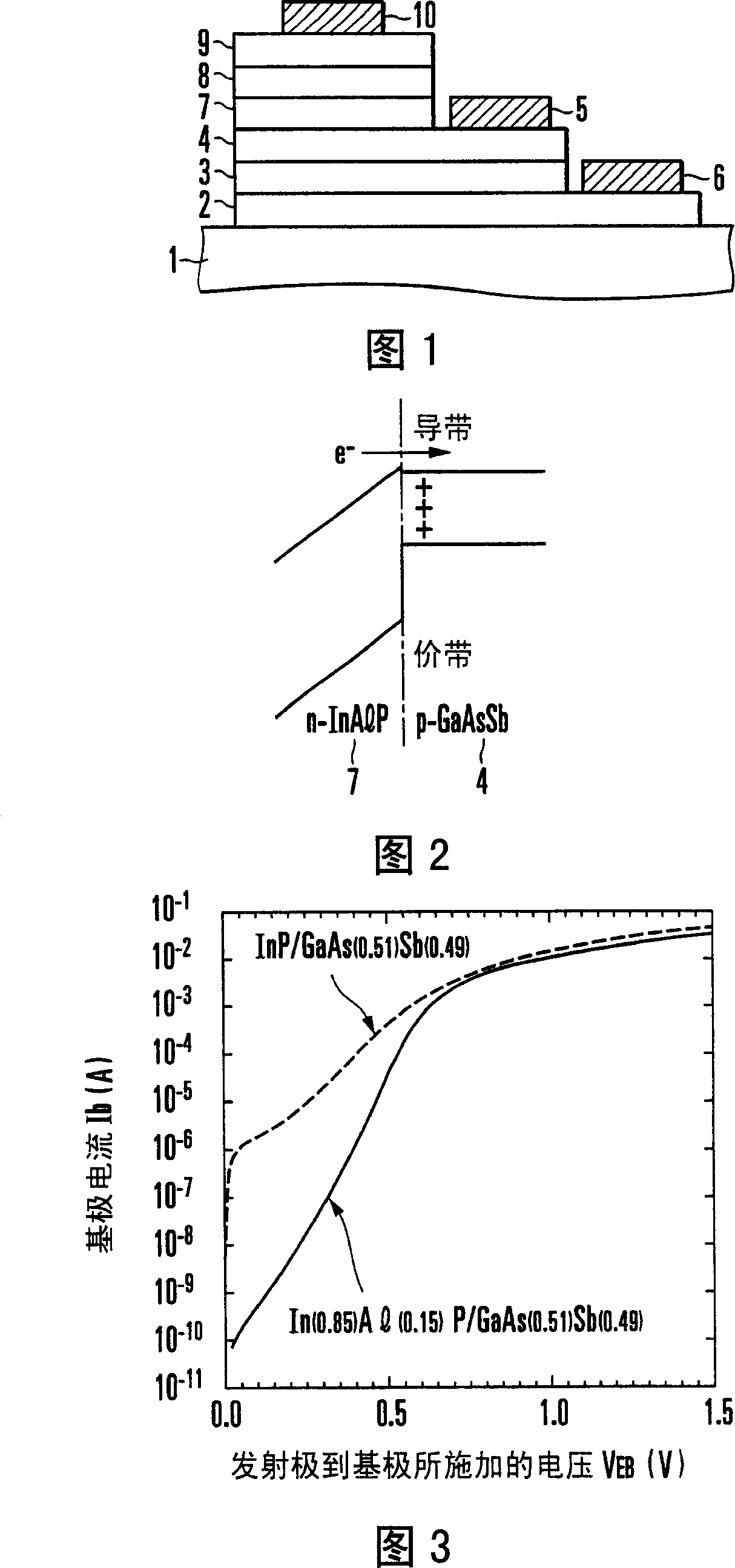
[0037] FIG. 1 is a schematic cross-sectional view showing an example of the arrangement of a heterostructure bipolar transistor according to an embodiment of the present invention. In this heterostructure bipolar transistor shown in Fig. 1, the n-type InP sub-collector layer 2 heavily doped with silicon (Si), the InP collector layer 3, and the n-type InP sub-collector layer 3 heavily doped with carbon (C) p-type GaAs (0.51) Sb (0.49) Base layer 4, n-type In doped with Si (1-y) Al (y) P emitter layer 7, n-type InP capping layer 8 heavily doped with Si, and n-type In heavily doped with Si (0.53) Ga (0.47) As contact layer 9 is stacked on InP substrate 1 which has increased resistance due to doping with iron (Fe) as an impurity and has a (100) main surface.

[0038] In addition, an ohmic-contact collector electrode 6 is formed on a region of the sub-collector layer 2 where ...


PUM


Abstract

An n-type InP sub collector layer 2 heavily doped with silicon (Si), an InP collector layer 3, a p-type GaAs(0.51)Sb(0.49) base layer 4 heavily doped with carbon (C), an n-type In(1-y)Al(y)P emitter layer 7 doped with Si, an n-type InP cap layer 8 heavily doped with Si, and an n-type In(0.53)Ga(0.47). As contact layer 9 heavily doped with Si are stacked on a substrate 1.

Description

technical field [0001] The invention relates to a heterostructure bipolar transistor having a base composed of GaAsSb. Background technique [0002] As a compound semiconductor used as a base layer material of an InP-based heterostructure bipolar transistor (HBT), GaAsSb is attracting attention. GaAsSb through mixture GaAs (0.51) Sb (0.49) Lattice matched to InP substrate. InP / GaAs using GaAsSb as base (0.51) Sb (0.49) / InP-based HBT can achieve good high-frequency characteristics and high breakdown voltage characteristics at the same time (Reference 1: "300 GHz InP / GaAsSb / InP Double HBTs with HighCurrent Capability and BVceo ≥ 6V", M.W.Dvorak, Student Member, IEEE, C.R. Bolognesi, Member, IEEE, O.J. Pitts, and S.P. Watkins, Member, IEEE,: IEEE ELECTRON DEVICE LETTERS, VOL.22, NO.8, AUGUST 2001 p.361). Heterostructures include Type I heterostructures and Type II heterostructures. In Type I heterostructures, the conduction band E of semiconductor A CA and valence band ...

Claims


Application Information

Patent Timeline
Patent Type & Authority Applications(China)
IPC IPC(8): H01L21/331H01L29/737
Inventor 小田康裕栗岛贤二横山春喜小林隆
Owner NIPPON TELEGRAPH & TELEPHONE CORP
Why Eureka
Try Eureka