Organic LED based on anode modification

Inactive Publication Date: 2007-06-20
INST OF CHEM CHINESE ACAD OF SCI
View PDF0 Cites 23 Cited by
  • Summary
  • Abstract
  • Description
  • Claims
  • Application Information

AI Technical Summary

Problems solved by technology

But this method requires a thicker film, which brings higher cost and affects the light transmission of the anode
The introduction of functional groups in the hole transport layer, or the assembly of functional molecular layers can also achieve the effect of hole injection enhancement (1: Hanson, E.L.; Guo, J.; Koch, N.; Schwartz, J.

Method used


Image

  • Organic LED based on anode modification
  • Organic LED based on anode modification
  • Organic LED based on anode modification

Examples


Embodiment 1

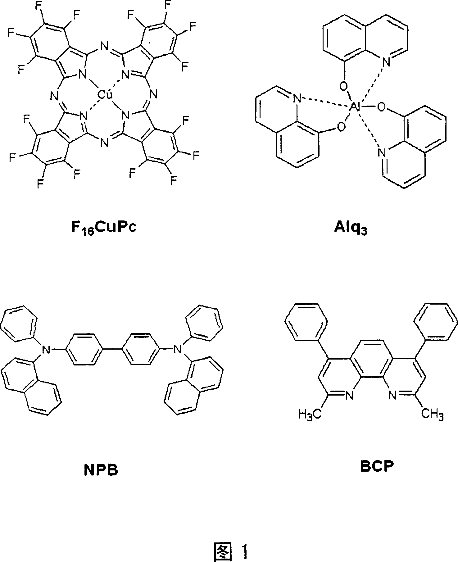
[0040] What shown in Fig. 1 is to be used to prepare the molecular formula of organic material of the present invention, be respectively strong electron-withdrawing molecule hexadecafluorophthalocyanine copper (F 16 CuPc), electron transport materials and luminescent materials 3-(8-hydroxyquinoline) aluminum (Alq 3 ), the hole-transporting material 4,4-2[N-(1-naphthalene)-N-aniline]bisphenyl (NPB) and the hole-blocking material 2,9-dimethyl-4,7-diphenyl- 1,10-Phenanthroline (BCP).

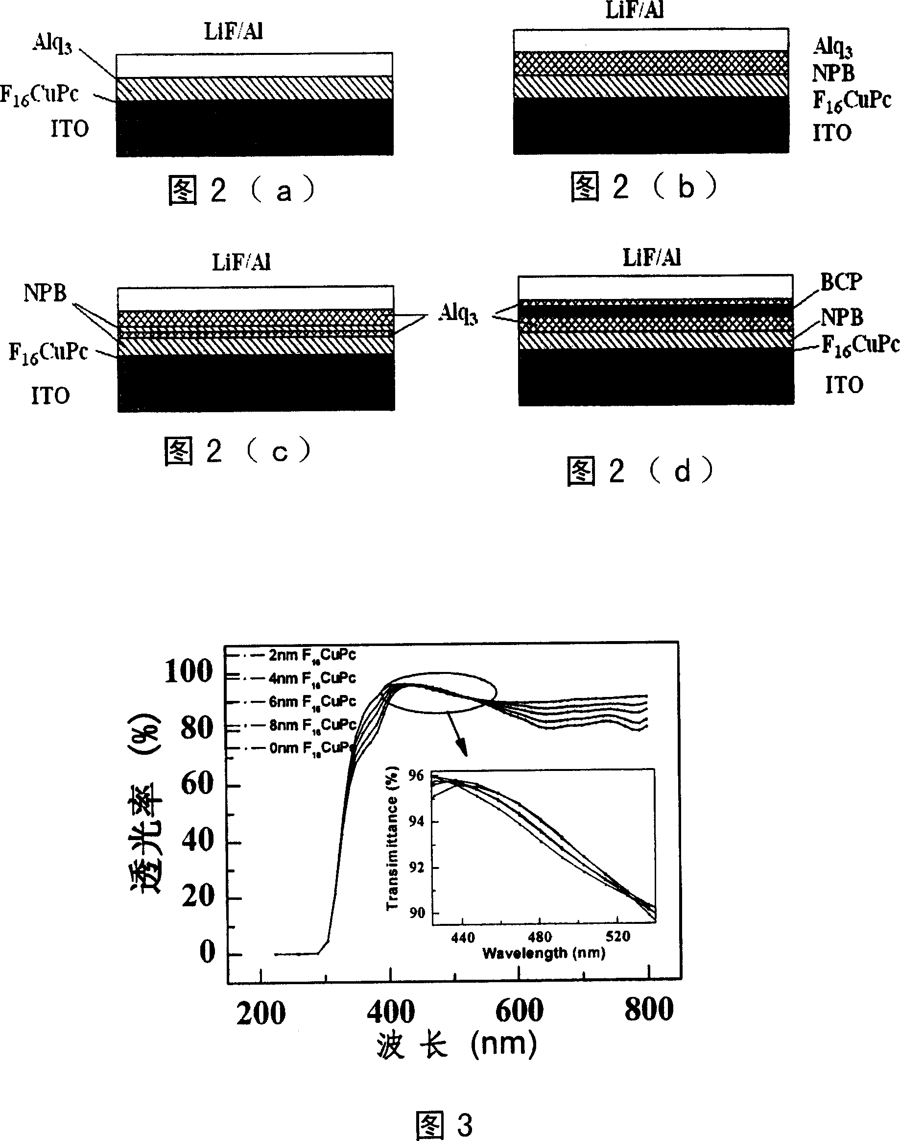
[0041] An organic light emitting diode structure of the present invention sequentially includes a substrate, a transparent bottom electrode of indium tin oxide (ITO), an organic layer and a cathode. The substrate can be made of the following materials: glass, ceramics, polymers, etc. The organic layer can be single layer, double layer and multilayer. The cathode is used for injection of electrons, and the electrode is made of a material with a low work function. It can be one metal or multiple ...

Embodiment 2

[0055] Prepared by the method of Example 1, the only difference is that the organic layer is a double-layer structure (NPB / Alq 3 ) (as shown in Figure 2b), both layers are 50nm. A low turn-on voltage (brightness up to 1cd / m 2 Voltage) of organic light-emitting diodes, the minimum turn-on voltage is 2.53V, reaching 100cd / m 2 The minimum voltage is 3.9V.

[0056] Fig. 5 is a graph showing current density-voltage, luminance-voltage and efficiency-current density curves of an organic light-emitting diode with a double organic layer structure according to the present invention.

[0057] Figure 6 is the surface atomic force microscope image of ITO and ITO / 4,4-2[N-(1-naphthalene)-N-aniline]biphenyl (NPB) before and after anode modification, wherein Figure 6a is ITO and Figure 6b is ITO / copper hexadecafluorophthalocyanine (F 16 CuPc), Figure 6c is ITO / NPB, Figure 6d is ITO / F 16 CuPc / NPB.

Embodiment 3

[0059] Prepared according to the method of Example 1, the only difference is that the organic layer is a multilayer structure, and the device structure is ITO / F 16 CuPc(4nm) / NPB(45nm) / Alq 3 (5nm) / NPB(5nm) / Alq 3 (45nm) / LiF / Al (as shown in Figure 2c). Obtained organic light-emitting diodes with high efficiency and low turn-on voltage, the highest efficiency is 7.63cd / A, and the turn-on voltage is 2.9V, reaching 100cd / m 2 The minimum voltage is 4.3V.


PUM


Abstract

The invention is concerned with the organic light emitter diode based on anode decoration, it is: deposits forced electronic molecular layer formed by hexadeca fluoro copper phthalocyanine on the indium tin oxide anode of the organic light emitter diode in order to forming the full dipole layer, constructs each function layer of the organic light emitter diode respectively on the forced electronic molecular layer, at least one of the function layer is with organic film and cathode. The invention is low cast, high light effect and lower operating voltage. The invention is also concerned with the decoration method of the organic light emitter diode based on anode decoration, that is simple operation, can use for several parts structure and with high light-admitting quality especially for blue and green light.

Description

technical field [0001] The invention relates to the technical field of light-emitting diodes, in particular to a novel anode modification method and an organic light-emitting diode structure with high efficiency and low operating voltage. Background technique [0002] Since U.S. Kodak Company (Tang, C.W.; Vanslyke, S.A.Appl.Phys.Lett.1987,51,913.) and British Cambridge University (Burroughs, J.H.; Jones, H.Nature1990,335,137.) invented efficient organic and Since the polymer electroluminescent device, organic light-emitting diodes have made great progress in performance and industrialization. High efficiency and low operating voltage have always been the goal that people are pursuing. At present, people use various methods such as synthesis and device structure to achieve this goal. Among them, the electrode modification of the device is an extremely important part, because it can be used without changing the material. Under the circumstances, the operating voltage is great...

Claims


Application Information

Patent Timeline
IPC IPC(8): H01L51/50H01L51/52H01L51/56
Inventor 于贵狄重安刘云圻徐新军朱道本
Owner INST OF CHEM CHINESE ACAD OF SCI
Why Eureka
Try Eureka