Transparent electrodes and electronic devices including the same

a technology of transparent electrodes and electronic devices, which is applied in the direction of carbon-silicon compound conductors, semiconductor devices, material nanotechnology, etc., can solve the problems of limited conductivity and flexibility of ito as currently used, cost issues, etc., and achieves improved light transmission, reduced sheet resistance, and suitable mechanical flexibility

Active Publication Date: 2018-06-19
SAMSUNG ELECTRONICS CO LTD
View PDF75 Cites 2 Cited by
  • Summary
  • Abstract
  • Description
  • Claims
  • Application Information

AI Technical Summary

Benefits of technology

[0009]An exemplary embodiment provides a transparent electrode, which provides enhanced mechanical flexibility, while having an improved conductivity and improved light transmission.
[0026]According to an exemplary embodiment, it is possible to provide a transparent electrode having suitable mechanical flexibility, while having a reduced sheet resistance and an improved light transmission.

Problems solved by technology

However, in view of application to a flexible touch panel or an Ultra Definition (UD) resolution display, ITO as currently used has limits in its conductivity and flexibility and also has a cost issue because of limited reserves of indium, so many attempts has been made to replace indium.

Method used


Image

  • Transparent electrodes and electronic devices including the same
  • Transparent electrodes and electronic devices including the same
  • Transparent electrodes and electronic devices including the same

Examples


example 1

[0125]A transparent electrode of Example 1 may be manufactured by the following method.

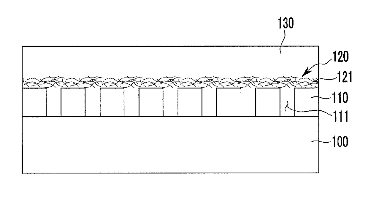
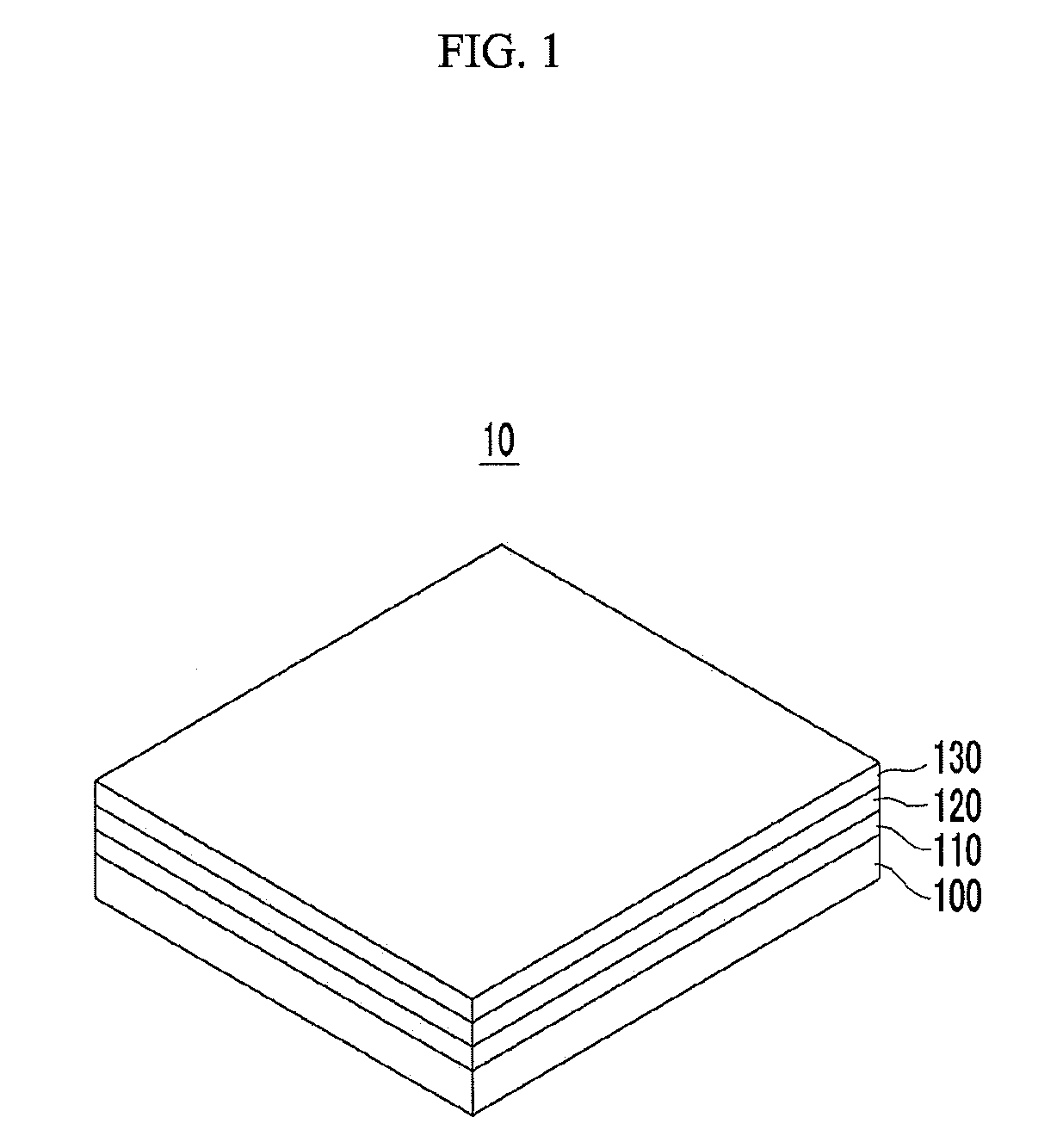
[0126][1] A graphene monolayer is deposited on one surface of a copper (Cu) foil by a chemical vapor deposition (CVD) method. After a polymethyl methacrylate (hereinafter, PMMA) layer is formed on the deposited graphene monolayer, the copper foil is removed by etching. Then, a PET-graphene monolayer stacked body may be obtained by transferring the graphene monolayer on which the PMMA layer has been formed on a PET substrate, and then the PMMA layer is removed.

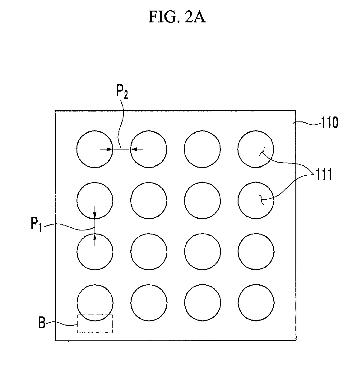
[0127][2] Then, a photoresist layer is formed on the graphene monolayer in the PET-graphene monolayer stacked body, and then is exposed and developed by disposing a mask including circular hole patterns on the photoresist layer. Then, a first layer, which is a first conductive layer including a graphene mesh structure may be formed on the PET substrate by removing the residual photoresist and then etching the graphene monolayer along the deve...

example 2

[0135]A transparent electrode is manufactured by an identical method to that of Example 1 except that a first layer including a graphene mesh structure, which is a first conductive layer, is formed on a substrate, and then about 3 mg of AuCl3 as a dopant and about 1 milliliter (mL) of nitromethane as solvent are mixed, and the thus-obtained mixture is doped onto the graphene mesh structure. A content of the doped AuCl3 is about 10 wt % with respect to a total weight of the first layer.

[0136]A sheet resistance of the graphene mesh structure doped with AuCl3, which is formed in Example 2 is measured by performing a four-point probe method on an upper surface thereof using the aforementioned LORESTA-GP MCP-T610 with ESP-type probes MCP-TP08P manufactured by MITSUBISHI CHEMICAL ANALYTECH, and the result thereof is shown in Table 1.

example 3

[0137]A transparent electrode is manufactured by the identical method to that of Example 1 except that a first layer including a graphene mesh structure, which is a first conductive layer is formed on a substrate, and then volatile HNO3 as a dopant is adsorbed and doped onto the graphene mesh structure in an atmosphere at a room temperature for about 10 minutes. A content of the doped HNO3 is about 0.01 wt % with respect to a total weight of the first layer.

[0138]A sheet resistance of the graphene mesh structure doped with HNO3, which is formed in Example 3, is measured by performing a four-point probe method on an upper surface thereof using the aforementioned LORESTA-GP MCP-T610 with ESP-type probes MCP-TP08P manufactured by MITSUBISHI CHEMICAL ANALYTECH, and the result thereof is shown in Table 1.

[0139]

TABLE 1Sheet ResistanceCoverage (%)Dopant(Ω / sq)Example 142Not Included1560Example 242AuCl3518Example 342HNO3337

[0140]Referring to Table 1, it can be seen that, in the case of Examp...


PUM

PropertyMeasurementUnit
sheet resistanceaaaaaaaaaa
widthaaaaaaaaaa
thicknessaaaaaaaaaa

Abstract

A transparent electrode includes a substrate; a first layer disposed on the substrate, the first layer including a graphene mesh structure, the graphene mesh structure including graphene and a plurality of holes; and a second layer disposed on the first layer, wherein the second layer includes a plurality of conductive nanowires.

Description

CROSS REFERENCE TO RELATED APPLICATIONS[0001]This application claims priority to and the benefit of Korean Patent Application No. 10-2015-0158426, filed in the Korean Intellectual Property Office on Nov. 11, 2015, and all the benefits accruing therefrom under 35 U.S.C. § 119, the entire contents of which are incorporated herein by reference.BACKGROUND[0002]1. Field[0003]The disclosed technology relates to a transparent electrode and an electronic device including the same.[0004]2. Description of the Related Art[0005]A flat display such as LCD, OLED, LED, and the like, and an electronic device such as a touch screen panel, a solar cell, a transparent transistor, and the like include a transparent electrode. A material for a transparent electrode desirably has a high light transmission, e.g., about 80% or more in a visible light range, and a low resistivity of, e.g., about 10−4 Ω*cm or less. An oxide material such as indium tin oxide (ITO), tin oxide (SnO2), zinc oxide (ZnO), or the l...

Claims


Application Information

Patent Timeline
Patent Type & Authority Patents(United States)
IPC IPC(8): H01L29/43H01L31/0224H01L29/16H01L29/167H01L33/42H01L29/45H01L29/41
CPCH01L29/1606H01L29/167H01L31/022466H01L29/41H01L29/413H01L29/43H01L29/45H01L33/42B82Y30/00H01B1/04H01B5/14
Inventor WOO, YUN SUNGSOHN, HIESANGSHIN, WEONHOCHO, EUN-HYOUNGKWAK, CHANPARK, HYEON CHEOLCHO, YOUNGJINKO, DONG-SUKO, WOONGKIM, KWANGHEE
Owner SAMSUNG ELECTRONICS CO LTD
Why Eureka
Try Eureka