Semiconductor structure

a semiconductor and structure technology, applied in the field of semiconductor structure, can solve the problems of deformation of the layer and its interface, deformation of the silicon photonic circuit, severe limitations on the thermal budget allowed for the integration and/or processing of devices, etc., to achieve the reduction of electrical and optical signals between the functional-oxide crystalline layer and the semiconductor substrate, and the flexibility and scope of application. , the effect of reducing the problem of decoupling electrical and optical signals

Active Publication Date: 2018-06-26
IBM CORP
View PDF4 Cites 0 Cited by
  • Summary
  • Abstract
  • Description
  • Claims
  • Application Information

AI Technical Summary

Benefits of technology

[0026]In the second configuration of an embodiment of the present invention, the functional oxide crystalline layer is preferably integrated within the interlayer dielectric layer thereby to be provided substantially in contact with one of: at least a crystalline surface of the semiconductor substrate and at least the optical aspect of the semiconductor substrate. Since the functional oxide crystalline layer may be provided with different possibilities relative to the semiconductor substrate and the electronic and optical aspects thereof, this feature may serve to broaden the flexibility and scope of application of an embodiment of the present invention. Where the functional-oxide crystalline layer is formed in contact with a given electronic device of the electronic aspect, such a device may be configured to drive a given active optical device in the functional-oxide crystalline layer.
[0027]Desirably, the interconnecting layer is processed to comprise at least a passive device configurable to electrically connect at least the active optical device of the functional-oxide crystalline layer to at least a given part of the semiconductor substrate. The interconnecting layer is processed to comprise metal interconnect levels that are configurable to electrically connect the functional-oxide crystalline layer to at least one of the electronic aspect and optical aspect and the afore-mentioned aspects to each other. Because substantially the same metal interconnect levels are used to make desired electrical connections, this feature imparts the advantages of ease of operation and fabrication to an embodiment of the present invention.
[0028]Preferably, an embodiment of the present invention is configurable to optically connect at least the active optical device of the functional-oxide crystalline layer to a given part of the semiconductor substrate with at least a given optical coupling technique. In addition to being electrically connected with the semiconductor substrate, the functional-oxide crystalline layer may also be optically coupled thereto. This can be done via a variety of different optical coupling techniques, such as, for example, evanescent coupling, grating coupling or other such suitable techniques. By using a dedicated optical coupling technique, the issues regarding decoupling electrical and optical signals between the functional-oxide crystalline layer and semiconductor substrate are reduced.
[0029]Preferably, the functional-oxide crystalline layer in an embodiment of the present invention comprises one of: a crystalline layer, a polycrystalline layer, a heterostructure and a superlattice. In this way, the compatibility of an embodiment of the present invention with well-established, cost-effective and mass-fabrication processing techniques is increased.
[0030]Desirably, an embodiment of the present invention is configurable to modify the given electro-optical property of the functional-oxide material with a given externally-applied stimulus. The functional-oxide material may be chosen on account of exhibiting specific electro-optical activity, optical non-linearities, optically driven metal-insulator transitions, which is tunable and / or modifiable with magnetic, optical, mechanical, stimuli. This feature may further enhance the performance and / or broaden the scope of application, versatility and performance of an embodiment of the present invention. In respect of this feature, and preferably, the functional-oxide crystalline layer is provided in relation to the interlayer dielectric layer so that the given electro-optical property is enhanced as desired. By a given integration of the functional-oxide crystalline layer in an embodiment of the present invention, for example, an orientation of the crystal axis versus electrodes, utilization of strain enhancement effects, the effect(s) of the given electro-optical property exhibited by the functional-oxide material may be further enhanced as desired.
[0031]Desirably, the interlayer dielectric layer in an embodiment of the present invention has a surface roughness of up to 1 nm. By way of this feature, the surface roughness of the second surface of the interlayer dielectric layer is relatively low so that the subsequent wafer-bonding of the functional-oxide crystalline layer thereon may be done with increased efficiency, reliability and quality.

Problems solved by technology

Whilst the use of such functional oxides in electro-optic modulators is known, integration within silicon photonic circuits has not yet been reported.
However, it is likely that such a layer and its interfaces would degrade when exposed to the relatively high temperatures used for FEOL processing, for example, during the activation anneal of the implanted source / drain region.
This approach may, however, suffer from severe limitations on the thermal budget allowed on the integration and / or the processing of devices based on functional oxides since BEOL processing temperatures are lower, for example, T<400° C., compared to the temperatures that may be used for obtaining functional oxides such as perovskites with desired electro-optical properties, typically 500° C. Also, the functional-oxide, crystalline layer would be spatially remote from the silicon photonic layer / circuitry fabricated during the FEOL, so that the optical coupling between the silicon photonics and the functional-oxide layer may be virtually impossible.

Method used


Image

  • Semiconductor structure
  • Semiconductor structure

Examples


Embodiment Construction

[0040]Within the description, the same reference numerals or signs have been used to denote the same parts or the like.

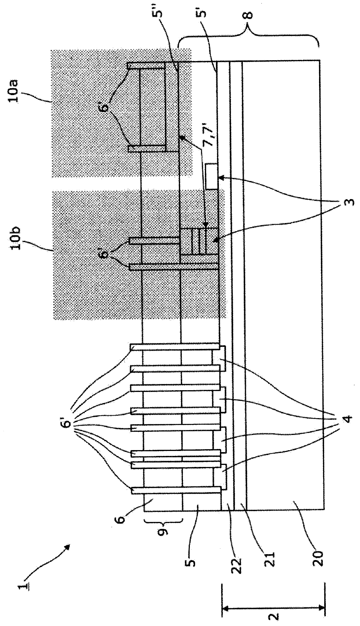
[0041]As can be seen from FIG. 1, a semiconductor structure 1 according to an embodiment of the present invention comprises a semiconductor substrate 2, which may be provided in a multi-layered configuration 20, 21, 22 of consecutively arranged layers of silicon 20, silicon dioxide 21 and a silicon substrate 22. The semiconductor substrate 2 is processed at a temperature of 700° C. to 1100° C. to comprise at least an optical aspect 3 comprising at least a silicon photonics device and at least an electronic aspect 4 comprising at least an electronic device 4. In the example shown in FIG. 1, the optical aspect 3 comprises multiple silicon photonic devices that are optical waveguides 3 and the electronic aspect 4 comprises multiple electronic transistors 4. On the processed semiconductor substrate 2, 3, 4, there is provided an interlayer dielectric layer 5—also known a...


PUM

PropertyMeasurementUnit
surface roughnessaaaaaaaaaa
temperatureaaaaaaaaaa

Abstract

A semiconductor structure is provided, the semiconductor structure comprising: a semiconductor substrate processed to comprise at least an optical aspect comprising at least a silicon photonics device and at least an electronic aspect comprising at least an electronic device; at least an interlayer dielectric layer provided on the semiconductor substrate, and at least an electrically interconnecting layer provided on the interlayer dielectric layer, wherein: the semiconductor structure further comprises at least a functional-oxide crystalline layer provided in relation to the interlayer dielectric layer before the interconnecting layer is provided on the interlayer dielectric layer, the functional-oxide crystalline layer comprising at least a functional-oxide material and is processed to comprise at least an active optical device, and the interlayer dielectric layer comprises a first surface and a second surface, the first surface being in common to at least a respective part of the optical aspect and the electronic aspect.

Description

CROSS-REFERENCE TO RELATED APPLICATION(S)[0001]This application is a continuation of U.S. application Ser. No. 14 / 945,752 filed on Nov. 19, 2015, now U.S. Pat. No. 9,696,488, which claims benefit of priority of U.K. Patent Application Number GB 1420531.4, filed on Nov. 19, 2014, the disclosures of which are incorporated by reference herein.TECHNICAL FIELD[0002]The present invention relates to a semiconductor structure and also extends to a method of fabricating such a structure.BACKGROUND[0003]Silicon photonics is a baseline technology that may be applicable for addressing a bandwidth bottleneck occurring in relation to future electronic circuits and / or systems. Silicon photonic circuits are based on many different elementary devices that may be applied for manipulating light. In a usual scenario, many of these elementary devices operate based on a change in the refractive index of one of their constituent materials, by applying an electrical field or current thereto.[0004]One of th...

Claims


Application Information

Patent Timeline
Patent Type & Authority Patents(United States)
IPC IPC(8): G02B6/12G02B6/13G02B6/122G02F1/035
CPCG02B6/122G02B6/13G02F1/035G02B2006/12142G02B2006/12047G02B2006/12061
Inventor ABEL, STEFANFOMPEYRINE, JEANMARCHIORI, CHIARA
Owner IBM CORP
Why Eureka
Try Eureka