Semiconductor device and method of forming the same

a semiconductor and semiconductor technology, applied in the direction of semiconductor devices, electrical devices, transistors, etc., can solve the problems of increased leakage current, difficult overall fabrication process and process control, and more limitations in the development process of planar fets

Active Publication Date: 2018-08-07
UNITED MICROELECTRONICS CORP
View PDF10 Cites 7 Cited by
  • Summary
  • Abstract
  • Description
  • Claims
  • Application Information

AI Technical Summary

Benefits of technology

[0008]Overall, the present invention provides an effective method of forming a semiconductor device, in which, a spacing layer is formed to simultaneously surround plural gates, and the spacing layer includes a dielectric material which may create a proper stress, such as a compressive stress nitride (SiN) or a tensile stress nitride. In this way, the spacing layer may be function like a compressive stress layer or a tensile stress layer, so as to create proper stress the channel regions below each the gates.

Problems solved by technology

However, as the size of the field effect transistors (FETs) is continuously shrunk, the development of the planar FETs faces more limitations in the fabricating process thereof.
While the foregoing method can improve the carrier mobility in the channel region, said method also has led to the difficulty of the overall fabrication process and the process control, especially under the trend of miniaturization of semiconductor device dimensions.
Thus, it is easy to cause some drawbacks, such as damages to the light doped drain (LDD) region leading to short channel effect, resulting in increased leakage current.

Method used


Image

  • Semiconductor device and method of forming the same
  • Semiconductor device and method of forming the same
  • Semiconductor device and method of forming the same

Examples


first embodiment

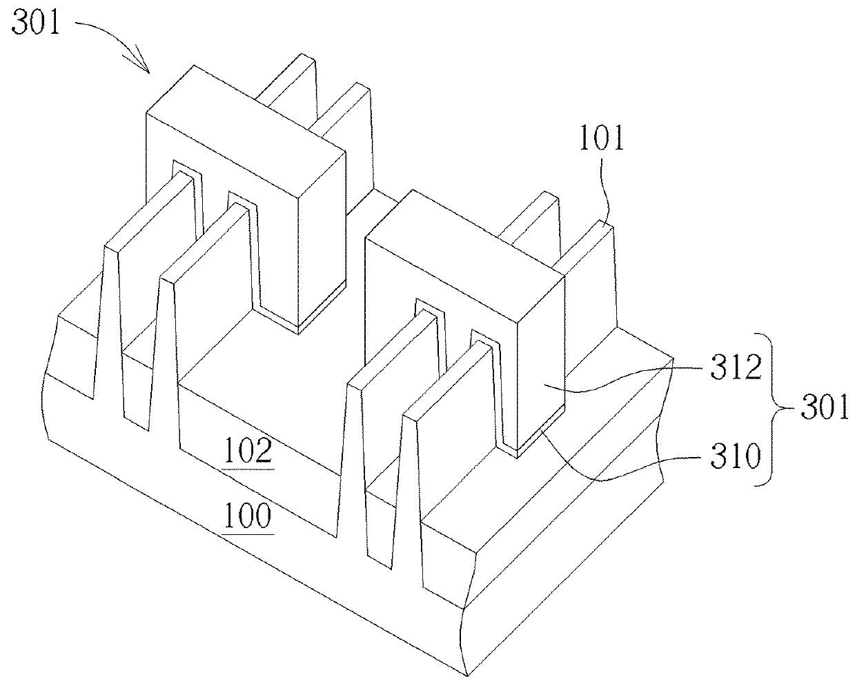
[0023]Please refer to FIG. 1 to FIG. 8, which are schematic diagrams illustrating a forming process of a semiconductor device according to the present invention. First of all, as shown in FIG. 1, a substrate layer 100 such as semiconductor substrate like silicon substrate, silicon containing substrate or silicon-on-insulator (SOI) substrate, is provided and at least one fin structures 101 is formed on a surface of the substrate 100.

[0024]In the embodiment of the bulk silicon, the fin structure 101 is formed through a sidewall image transfer (SIT) process. The process may include forming a plurality of patterned sacrificial layers (not shown in the drawings) on a bulk silicon substrate not shown in the drawings) by using a photolithography and an etching process, performing a depositing and an etching processes sequentially to form a spacer (not shown in the drawings) at sidewalls of each of the patterned sacrificial layers, and then removing the patterned sacrificial layers and perf...

fourth embodiment

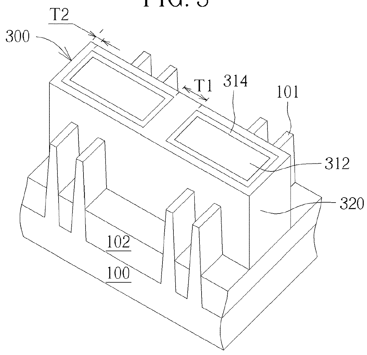
[0041]Please refer to FIG. 11, which are schematic diagrams illustrating a forming method of a semiconductor device according to the present invention. In the present embodiment, metal gate 400 is formed directly with the metal gate 400 includes a high dielectric constant (high-k) dielectric layer 410, a barrier layer (not shown in the drawings), a work function metal layer 412 and a metal gate layer 414 stacked one over another, and a spacer 416 surrounded the high-k dielectric layer 410, the barrier layer, the work function metal layer 412 and the metal gate layer 414. Then, the metal gate 400 is patterned to form two separated portions, with each portion thereof across a portion of the fin structures 101 respectively.

[0042]Following these, a sacrificial spacer (not shown in the drawings) simultaneously surrounded the two portions of the metal gate 400, two source / drain regions at two sides of each portion of the metal gate 400, and a ILD layer 200 covered the substrate 100 are fo...


PUM


Abstract

A semiconductor device and a method of forming the same, the semiconductor device includes a plural fin structures, two gates, a protection layer and an interlayer dielectric layer. The fin structures are disposed on a substrate. The two gates are disposed on the substrate across the fin structures. The protection layer is disposed on the substrate, surrounded sidewalls of the two gates. The interlayer dielectric layer is disposed on the substrate, covering the fin structures and the two gates.

Description

BACKGROUND OF THE INVENTION1. Field of the Invention[0001]The present invention relates to a semiconductor device and a forming method thereof, and more particularly to a semiconductor device having a stress layer and a forming method thereof.2. Description of the Prior Art[0002]With increasing miniaturization of semiconductor devices, it is crucial to maintain the efficiency of miniaturized semiconductor devices in the industry. However, as the size of the field effect transistors (FETs) is continuously shrunk, the development of the planar FETs faces more limitations in the fabricating process thereof. On the other hand, non planar FETs, such as the fin field effect transistor (FinFET) have three-dimensional structure, not only capable of increasing the contact to the gate but also improving the controlling of the channel region, such that the non planar FETs have replaced the planar FETs and become the mainstream of the development.[0003]For the sake of increasing the carrier mob...

Claims


Application Information

Patent Timeline
Patent Type & Authority Patents(United States)
IPC IPC(8): H01L21/00H01L21/02H01L21/8234H01L29/66H01L21/8238H01L29/78H01L27/02H01L29/08H01L27/092H01L27/00H01L29/00
CPCH01L27/0924H01L27/0207H01L29/0847H01L29/7843H01L21/823821H01L21/823828H01L29/6653H01L21/823418H01L21/02636H01L29/785H01L21/823857
Inventor LEE, RUNG-YUANTUNG, YU-CHENGLU, CHUN-TSENLIOU, EN-CHIUANCHEN, KUAN-HUNG
Owner UNITED MICROELECTRONICS CORP
Why Eureka
Try Eureka