System and method for cryogenic optoelectronic data link

Active Publication Date: 2018-10-09
SEEQC INC
View PDF260 Cites 12 Cited by
  • Summary
  • Abstract
  • Description
  • Claims
  • Application Information

AI Technical Summary

Benefits of technology

[0051]Kalugin, Nikolai G., et al. “Graphene-based quantum hall effect infrared photodetectors.”SPIE OPTO. International Society for Optics and Photonics, 2012.
[0052]A quantum stark effect modulator or sensor may also be employed, using a grapheme layer heterostructure. Liu, Ming, et al. “A graphene-based broadba

Problems solved by technology

These devices are low in power, and can output f

Method used


Image

  • System and method for cryogenic optoelectronic data link
  • System and method for cryogenic optoelectronic data link
  • System and method for cryogenic optoelectronic data link

Examples


Embodiment Construction

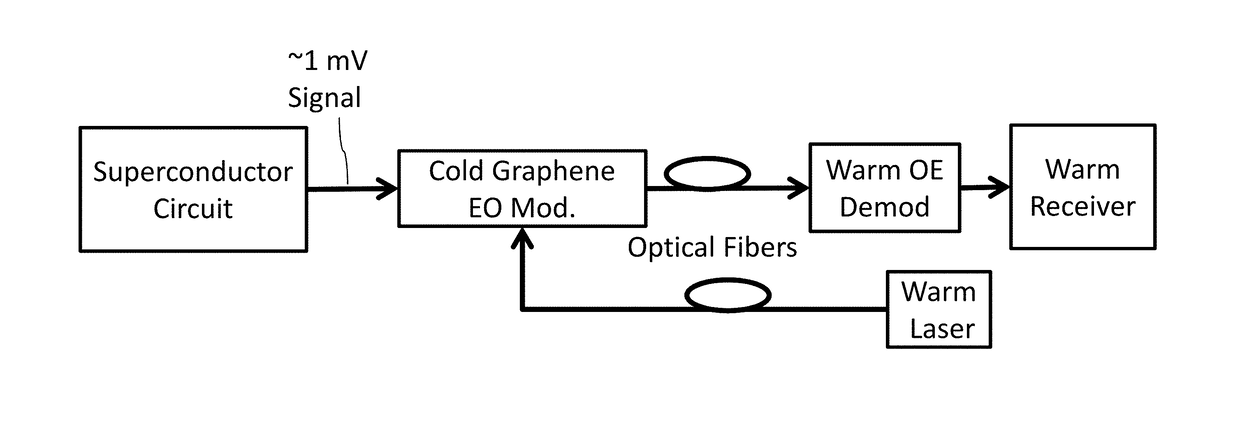
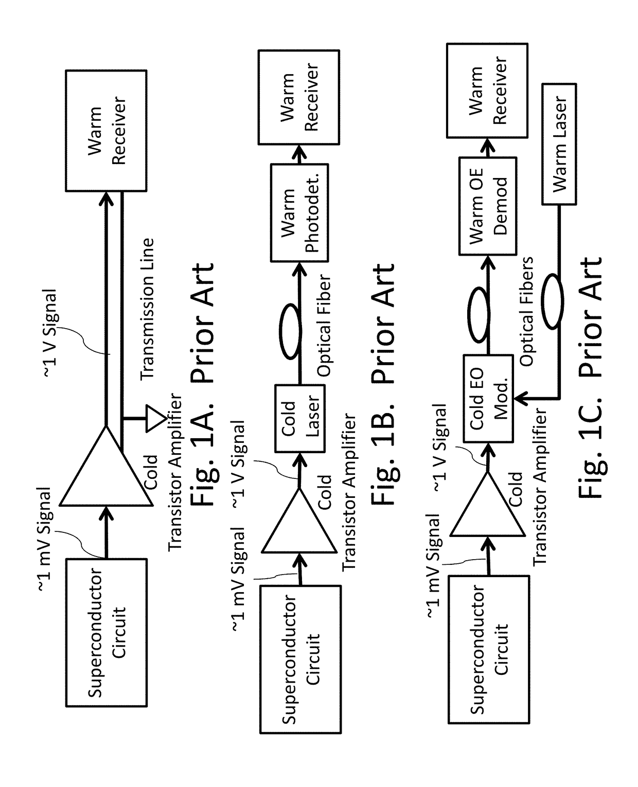
[0092]The present technology may be used to provide an external interface for a superconducting circuit comprising an ultrafast microprocessor that generates 64-bit digital words at a clock rate of 25 GHz, at a temperature of 4 K. Such a circuit could be designed using Rapid-Single-Flux-Quantum (RSFQ) logic, or one of its low-power alternatives known as Reciprocal Quantum Logic (RQL), Energy-Efficient RSFQ, or Quantum Flux Parametron. See, for example, U.S. Pat. No. 8,571,614; U.S. Pat. No. 7,843,209; U.S. Pat. No. 7,786,748.

[0093]Logic gates in these technologies exhibit switching energies of order 10−18 J / gate, corresponding to signal levels of order 1 mV and 0.5 mA for 2 ps. For a chip with one million gates at a clock rate of 25 GHz, this corresponds to a total power dissipation of 25 mW. The power associated with input / output lines and drivers at 4 K should be comparable to this. Taking a 64-bit data bus from 4 K to room temperature, 25 mW corresponds to 0.015 pJ / bit, an extrem...


PUM


Abstract

A cryogenic optoelectronic data link, comprising a sending module operating at a cryogenic temperature less than 100 K. An ultrasensitive electro-optic modulator, sensitive to input voltages of less than 10 mV, may include at least one optically active layer of graphene, which may be part of a microscale resonator, which in turn may be integrated with an optical waveguide or an optical fiber. The optoelectronic data link enables optical output of weak electrical signals from superconducting or other cryogenic electronic devices in either digital or analog form. The modulator may be integrated on the same chip as the cryogenic electrical devices. A plurality of cryogenic electrical devices may generate a plurality of electrical signals, each coupled to its own modulator. The plurality of modulators may be resonant at different frequencies, and coupled to a common optical output line to transmit a combined wavelength-division-multiplexed (WDM) optical signal.

Description

CROSS REFERENCE TO RELATED APPLICATIONS[0001]The present application is a non-provisional of, and claims benefit of priority from U.S. Provisional Patent Application No. 62 / 256,991, filed Nov. 18, 2015, the entirety of which is expressly incorporated herein by reference.BACKGROUND OF THE INVENTION[0002]There are several low-power cryogenic electronic technologies that require broadband communication of analog or digital data to conventional electronic systems at room temperature. These include ultrafast superconducting circuits for data conversion, radio communications, and computing, as well as superconducting circuits for quantum computing and sensitive imaging arrays across the electromagnetic spectrum. A key problem with these systems is that the characteristic voltage output of these low-power systems is 1 mV or even less, while room-temperature semiconductor electronic devices have a typical voltage level of order 1 V or more. In some cases, one can use a high-gain transistor ...

Claims


Application Information

Patent Timeline
IPC IPC(8): G02F1/035H04B10/80H04B10/556H04B10/516H04J14/02H04B10/69H04B10/54
CPCH04B10/80H04B10/5563H04B10/5161H04J14/02H04B10/69H04B10/541H04B10/505
Inventor VERNIK, IGOR V.MUKHANOV, OLEG A.KADIN, ALAN M.PHARE, CHRISTOPHER THOMASLIPSON, MICHALBERGMAN, KEREN
Owner SEEQC INC
Why Eureka
Try Eureka