
Plasma processing method

a processing method and plasma technology, applied in the field of plasma processing methods, can solve problems such as process fluctuation (fluctuation in the chamber atmosphere) and achieve the effects of suppressing process fluctuation in plasma etching, removing residues, and stabilizing the atmospher

Active Publication Date: 2019-01-22
HITACHI HIGH-TECH CORP
View PDF12 Cites 2 Cited by
  • Summary
  • Abstract
  • Description
  • Claims
  • Application Information

AI Technical Summary

Benefits of technology

The patent describes a process that can remove any residue from plasma cleaning, stabilize the atmosphere in a chamber, and prevent fluctuations during plasma etching.

Problems solved by technology

It is a problem that process fluctuation (fluctuation in the chamber atmosphere) occurs in etching due to deposition of a residue (residual gas) caused by the plasma cleaning in the chamber.

Method used


Image

  • Plasma processing method
  • Plasma processing method
  • Plasma processing method

Examples


embodiment 1

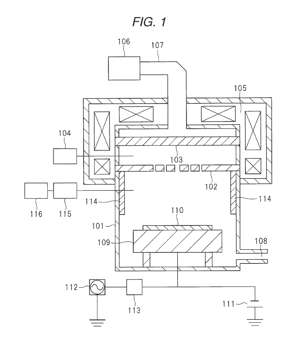
[0020]FIG. 1 is a sectional view illustrating an example of a schematic structure of a plasma processing apparatus according to Embodiment 1 of the invention.

[0021]Hereinafter, the plasma processing apparatus of Embodiment 1 will be described. The plasma processing apparatus illustrated in FIG. 1 is a microwave Electron Cyclotron Resonance (ECR) plasma etching apparatus which is an example thereof. Here, an electrode that is provided inside a processing chamber 101, an electric field that is provided outside a chamber, a supply device of a magnetic field, power supply, or the like are schematic illustrated.

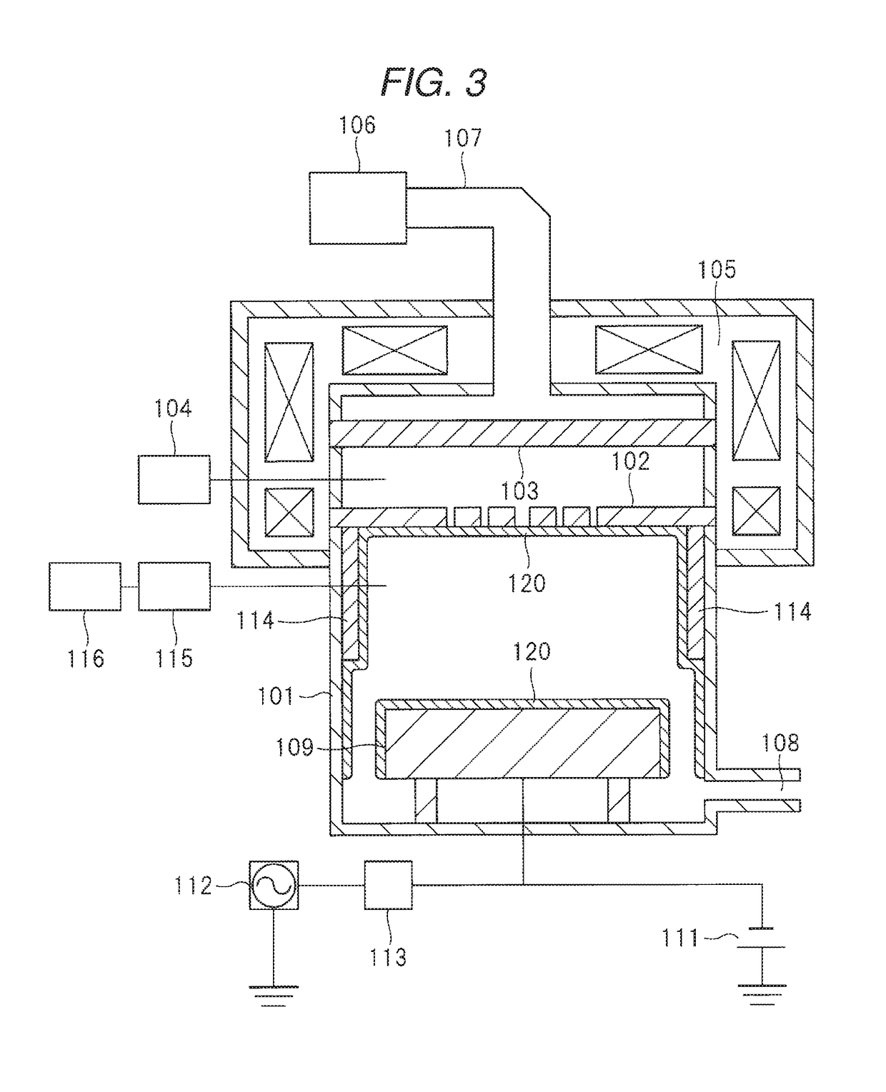
[0022]A configuration of the plasma processing apparatus of Embodiment 1 illustrated in FIG. 1 will be described. The plasma processing apparatus includes the processing chamber 101 which includes a chamber in which plasma etching processing is performed with respect to a sample 110 such as a semiconductor substrate and of which an upper portion is opened. A disk-shaped shower pla...

embodiment 2

[0054]FIG. 7 is a flowchart illustrating an example of a procedure of a plasma processing method according to Embodiment 2 of the invention.

[0055]Since a plasma processing apparatus of Embodiment 2 is the same as the plasma processing apparatus illustrated in FIG. 1 described in Embodiment 1, duplicate description of the structure thereof will be omitted.

[0056]Next, the plasma processing method of Embodiment 2 will be described with reference to FIG. 7.

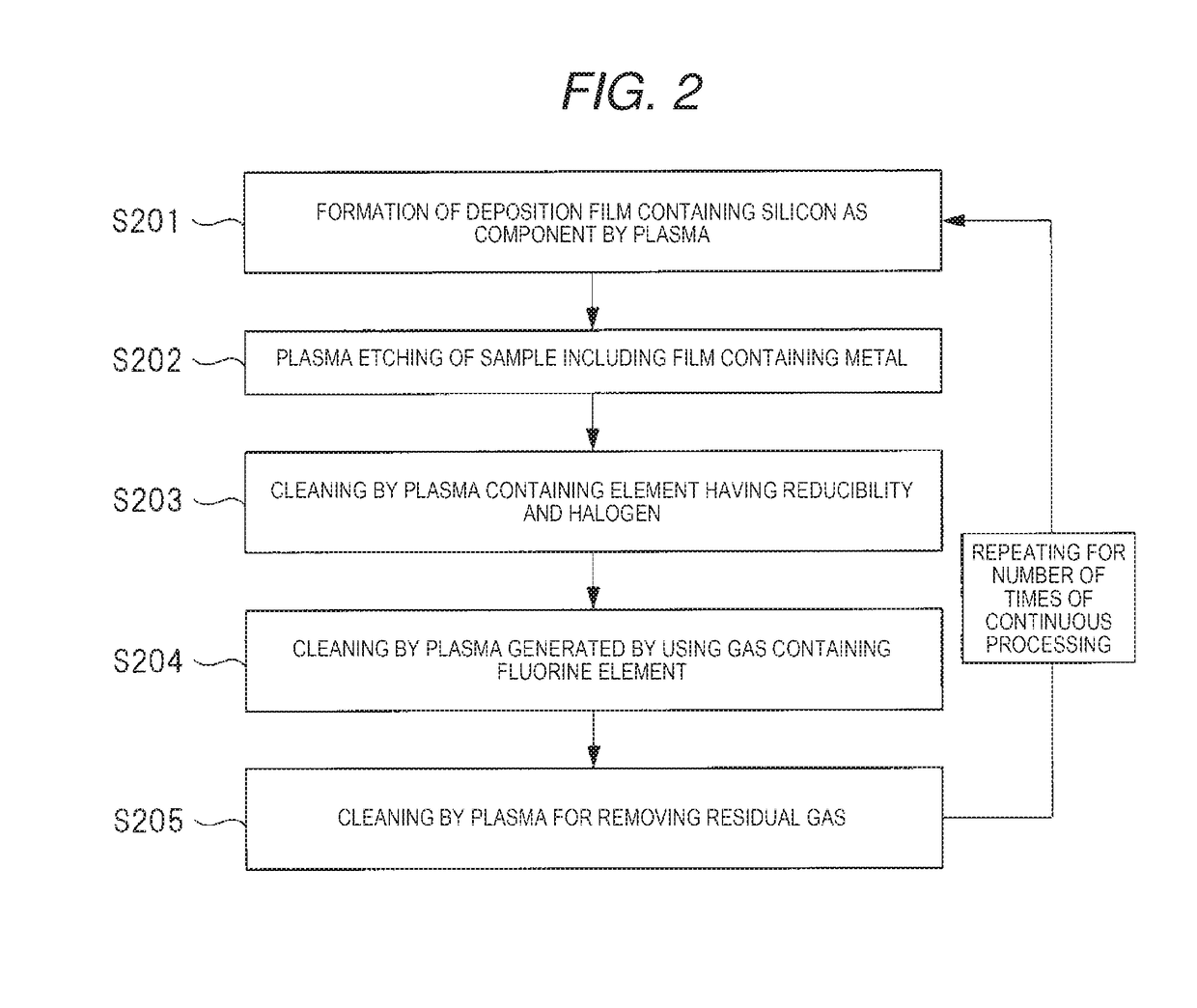
[0057]The plasma processing method according to Embodiment 2 is configured of six elements (steps) of (1) to (6) illustrated below and is processed in accordance with the procedure illustrated in FIG. 7. That is, (1) forming of a deposition film containing silicon as a component by using plasma, (2) plasma etching of a sample having a film containing a metal, and (3) cleaning by an element having reducibility and plasma containing halogen. Furthermore, (4) cleaning by plasma for removing residual element having reducibility, (5) clean...


PUM

PropertyMeasurementUnit
pressureaaaaaaaaaa
pressureaaaaaaaaaa
pressureaaaaaaaaaa

Abstract

A plasma processing method includes forming a deposition film containing silicon as a component in a processing chamber by generating a first plasma in the processing chamber; plasma etching of a sample in which a film containing a metal is formed in the processing chamber; and removing of a metal-based reaction product by generating a second plasma including an element having reducibility and halogen. The plasma processing method further includes removing the deposition film by a third plasma generated by using gas containing a fluorine element; and removing residual gas by a fourth plasma.

Description

BACKGROUND OF THE INVENTIONField of the Invention[0001]The present invention relates to a plasma processing method such as cleaning using plasma.Background Art[0002]In recent years, a device structure has been complicated with miniaturization of a large-scale integrated circuit and demands for machining accuracy and stability in an etching step are getting stricter. A factor of process fluctuation in the etching step includes a temperature change of a member in a chamber or the like, accumulation of a reaction product generated by etching processing, or the like.[0003]In addition, in a Metal Oxide Semiconductor Field Effect Transistor (MOSFET), a metal gate / High-k structure using a metal material for a gate electrode and a High-k material (hafnium oxide film or the like) for a gate insulating film becomes a mainstream with the miniaturization thereof. Due to the appearance of the metal gate / High-k structure, various types of metal etching are required. Accumulation of a metal-based ...

Claims


Application Information

Patent Timeline
Patent Type & Authority Patents(United States)
IPC IPC(8): C23C16/24C23C16/50C23C16/44C23C16/455C23C16/448
CPCC23C16/24C23C16/4404C23C16/50C23C16/4485C23C16/45557C23C16/4405C23C16/507H01L21/32136H01L21/02274H01L21/02315H01L21/0234H01L21/3065
Inventor YONEMOTO, TAKAHIROSUMIYA, MASAHIROKAMAJI, YOSHITOSASAKI, JUNYA
Owner HITACHI HIGH-TECH CORP
Learn More