
Method for the synthesis of layered luminescent transition metal dichalcogenide quantum dots

a luminescent transition metal and quantum dots technology, applied in the field of synthesis of layered luminescent transition metal dichalcogenide quantum dots, can solve the problems of inability to use graphene in optical/electronic applications, inability to synthesis and characterization of mossub>2 /sub>nanoclusters, and infancy of methods, etc., to achieve fast growth of mos2, cost-effective and eco-friendly, and simple and cost-effectiv

Inactive Publication Date: 2019-04-16
INDIAN INST OF SCI EDUCATION & RES THIRUVANANTHAPURAM IISER TVM
View PDF9 Cites 1 Cited by
  • Summary
  • Abstract
  • Description
  • Claims
  • Application Information

AI Technical Summary

Benefits of technology

[0029]One advantage of the present invention is its simplicity to synthesize the nanostructured materials via simple, cost effective, and green approach.
[0030]Another advantage of the present invention of the synthesized MX2 quantum dots is its use as high performance electrocatalysts for HER; for example, it can be used in solar water-splitting applications.
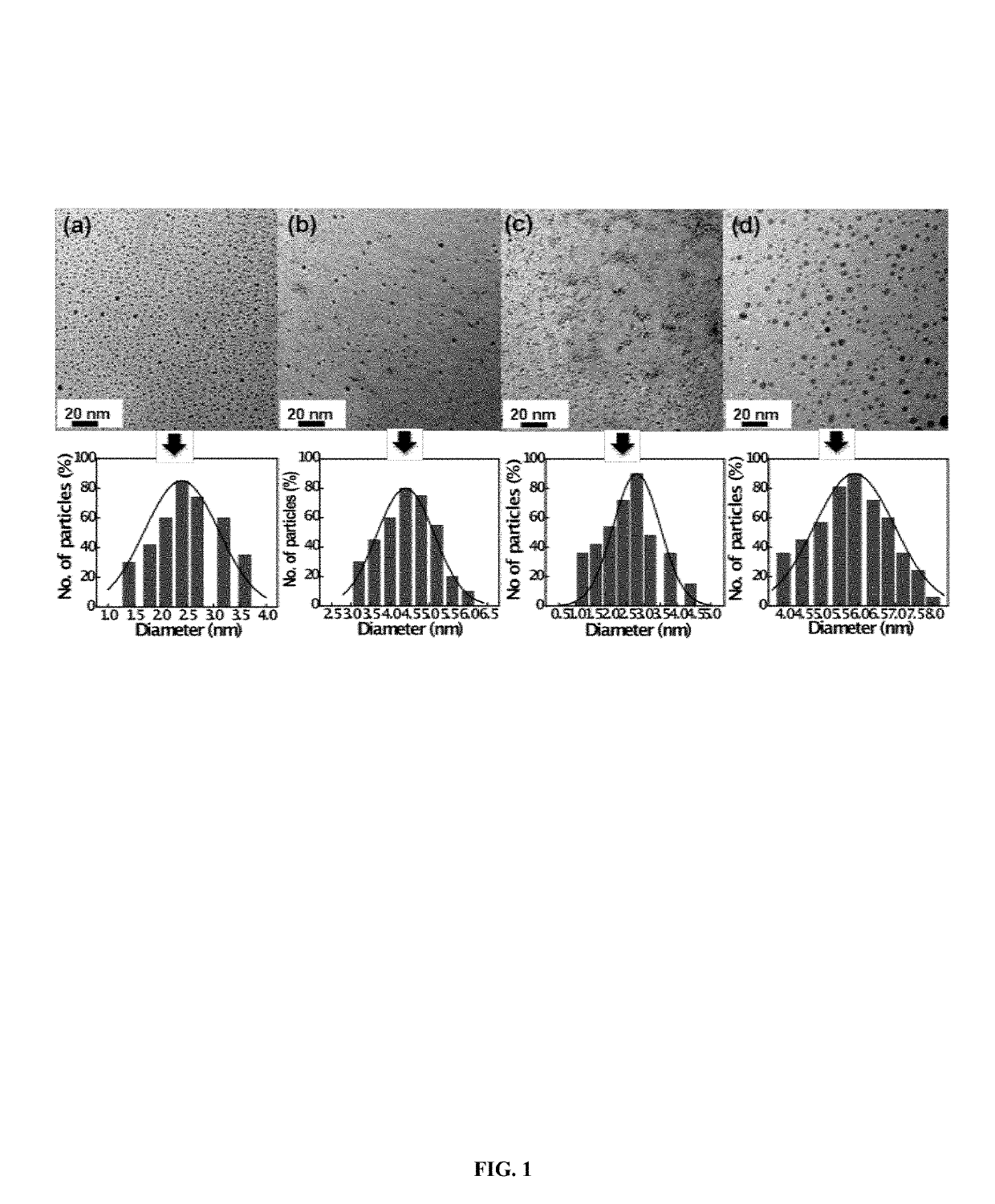
[0031]In an embodiment, the invention provides an effective method for a very fast growth of MoS2 and MoSe2 nanoclusters of various sizes. These clusters were obtained by applying a constant DC potential of 5V across LiTFSI or [BMIm]Cl of various concentrations viz. 0.1, 1 and 5 wt. %. The elelctrolyte solution may also include other materials to tailor the properties and size of the nanoclusters.
[0032]Another aspect of the invention is directed towards providing aq.—based very dilute electrolytes making the entire method cost effective and eco-friendly. The use of dilute aqeuous electrolyte and the application of the potential much higher than the electrochemical window of the electrolyte, leads to formation of exotic or reactive hydroxyl and oxygen free radicals triggering the exfoliation.
[0033]In another aspect of the invention, through a single-step method, these nanoclusters can be directly deposited onto any conducting substrate. Such electrodeposited materials can directly be used for various application as they show enhanced electrocatlaytic performance towards HER (water splitting), owing to the improved electronic conductivity and the emergence of new active sites.
[0034]In yet another embodiment of the invention MX2 discs (diameter 1 cm) made from commercially available flakes, were placed in an electrochemical cell in aq. LiTFSI or [BMIm]Cl of various concentrations viz. 0.1, 1 and 5 wt. %. A constant potential of 5V is applied to between the electrodes for a suitable time, at room temperature. In yet another embodiment, the electrolyte solution is reacted for a period of time from about 0.5 hour to about 5 hours. Furthermore, this solution was centrifuged and the supernatant solution was collected and analyzed further.

Problems solved by technology

Even though graphene exhibits numerous unusual physical properties and applications thereof, its semi-metallic nature disables graphene to be used in optical / electronic applications.
However, the synthesis and characterization of MoS2 nanoclusters is still in its infancy.
Previously reported methods are very tedious and / or yield polydisperse distribution of particles.
However, both these techniques fail in the large-scale exfoliation of TMDs.
However, in their approach, only a few layered sheets of graphene and MoS2 have been obtained.
As already known, extraction of materials from solvent exfoliation route is very difficult for any practical application.

Method used


Image

  • Method for the synthesis of layered luminescent transition metal dichalcogenide quantum dots
  • Method for the synthesis of layered luminescent transition metal dichalcogenide quantum dots
  • Method for the synthesis of layered luminescent transition metal dichalcogenide quantum dots

Examples


example 1

Electrochemical Exfoliation of MoS2 and MoSe2 and Preparation Method of the Luminescent Molybdenum Disulphide (MoS2) and Molybdenum Diselenide (MoSe2) Quantum Dots

[0042]Molybdenum disulfide (MoS2) and molybdenum diselenide (MoSe2) flakes, Ionic Liquids commercially available as LiTFSI salt, [BMIm]Cl from Sigma Aldrich, were used as received without any further purification. In a typical example, the electrolyte for the electrochemical exfoliation was prepared by mixing LiTFSI with de-ionized water (0.1 wt. % and 1 wt. %).

[0043]Pelletized MoS2 / MoSe2 discs made from commercially available flakes, were placed in an electrochemical cell with 1 cm apart in aq. LiTFSI or [BMIm]Cl of the following concentrations: 0.1, 1 and 5 wt. %. A constant potential of 5V was applied to between the electrodes for 3 hours, at 25° C. This solution was centrifuged for 1 h at 6000 rpm. The supernatant solution was collected and analyzed further. The method can be carried out using several other RTILs such ...

example 2

Direct Deposition of Molybdenum Diselenide (MoSe2) Quantum Dots onto Conducting Substrates

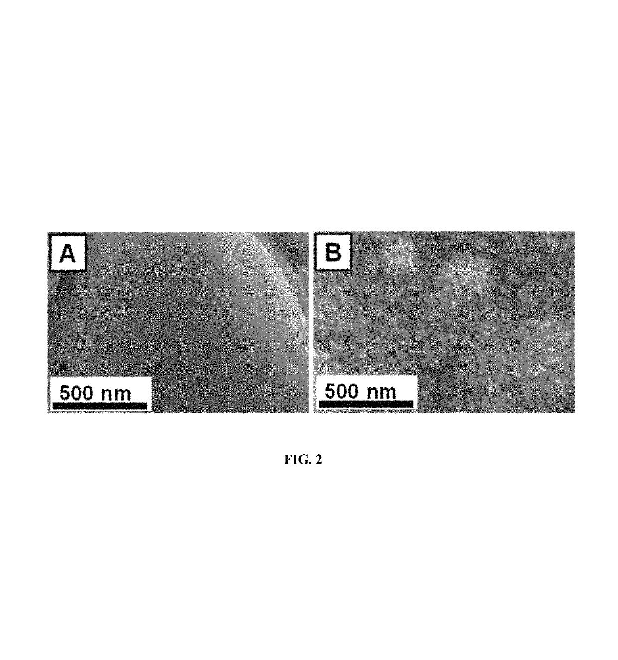
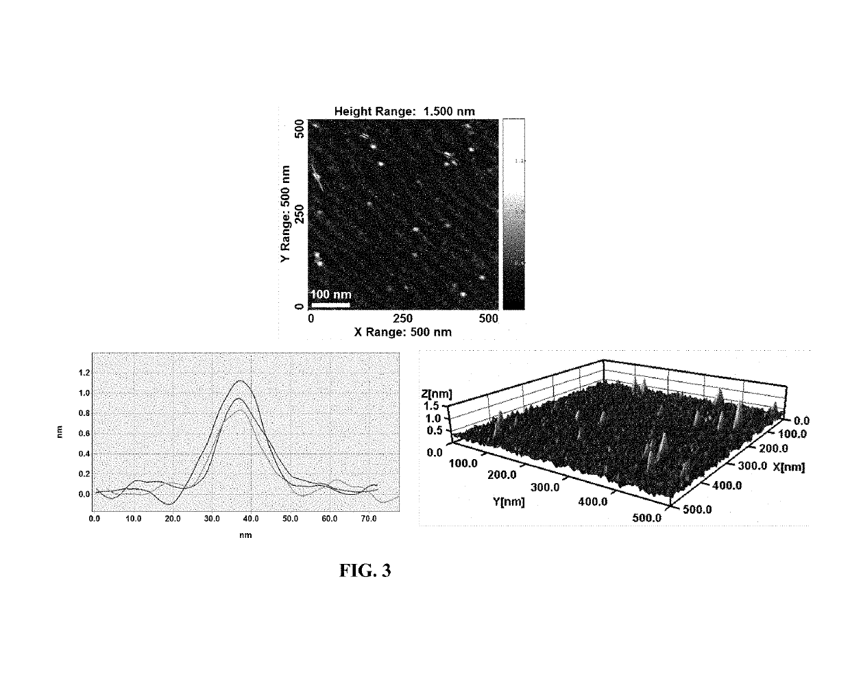
[0044]In yet another aspect of the present invention, electrochemical exfoliation method was employed for synthesizing MoSe2 nanocrystals, starting from their bulk, by using 0.1 wt % aq. LiTFSI electrolyte under a constant applied DC potential of 5 V. In a typical synthesis, 500 mg of MoSe2 powder was pelletized by applying a pressure of 5 tons / cm2. This pellet was employed as anode and conducting substrates of choice viz. gold, FTO or similar material can be used as cathode for the electrochemical exfoliation. The electrodes were placed in an electrochemical cell 1 cm apart, in 0.1 wt. % aq. LiTFSI electrolyte. The exfoliated electrolyte solution contains a mixture of several exfoliation / oxidation / decomposition products whose composition is much complex to elucidate. However, a drift of the exfoliation products towards the negative electrode was observed as the exfoliation proceeded and a unif...

example 3

Electrochemical Preparation of Quantum Dots of WS2 / WSe2 and Direct Deposition on Conducting Substrates for Energy Applications

[0045]Following similar protocols described in Example 1-3, quantum dots of WS2 / WSe2 is also synthesized and was directly deposited onto transparent conducting substrates / gold foil for energy harvesting or conversion applications. WS2 quantum dots are particularly interesting for electrocatalytic hydrogen evolution because of the favorable thermoneutral chemistry of metal / chalcogenide edges.

Electrochemical HER Measurements of MoS2 Quantum Dots

[0046]Electrochemical HER measurements were carried out using three-electrode cell with 0.5 M H2SO4 as electrolyte. As synthesized MoS2 quantum dots with 5 wt. % nafion solution was drop-casted onto glassy carbon electrode and dried at room temperature, which acts as working electrode. Pt wire auxiliary electrode and Ag / AgCl were used as counter and reference electrodes respectively. The performance of the catalyst towar...


PUM

PropertyMeasurementUnit
diameteraaaaaaaaaa
electric potentialaaaaaaaaaa
particle sizeaaaaaaaaaa

Abstract

The invention discloses a method for the synthesis of monodispersed luminescent quantum dots of transition metal dichalcogenides (TMDC), single- or few-layered, using a single-step electrochemical exfoliation that involves dilute ionic liquid and water. The method disclosed helps to obtain nanoclusters of TMDC of desired size including small sizes ranging up to 6 nm, by varying the concentration of the electrolyte and the applied DC voltage. The invention further discloses a method by which mono- or few-layered luminescent transition metal dichalcogenides can be directly deposited onto conducting substrates in a uniform manner. The monodispersed single- or few-layered luminescent TMDC and electro-deposited substrates exhibit improved electronic conductivity and new active sites, making them suitable as high-performance electrocatalysts in hydrogen evolution reactions in solar water-splitting applications and also as electrodes for solar cell applications.

Description

PRIORITY PARAGRAPH[0001]This application claims priority to Indian patent application No. 4004 / CHE / 2015 filed on Aug. 1, 2015 titled “A single step method for the synthesis of molybdenum disulfide quantum dots” and is incorporated herein by reference.BACKGROUND[0002]Experimental realization of ultrathin graphene nanosheets opened up a new horizon for the academic and applied research. Even though graphene exhibits numerous unusual physical properties and applications thereof, its semi-metallic nature disables graphene to be used in optical / electronic applications. Semi-conducting inorganic analogues of graphite-like transition metal dichalcogenides (TMDs) are one of the most attractive alternatives for such applications. Molybdenum disulfide (MoS2) is well studied and shows an interesting layered structure as well as unusual physical properties. Reports such as Applied Physics Letters 2013,102 (12), demonstrate that MoS2-based electronic devices out-perform graphene-based ones. Nano...

Claims


Application Information

Patent Timeline
Patent Type & Authority Patents(United States)
IPC IPC(8): C25B1/00C25B9/00C01G41/00C01G39/00C09K11/88C01G39/06C01B19/00B82Y30/00B82Y20/00B82Y40/00
CPCC25B1/00C01G39/00C01G39/06C01G41/00C09K11/881C25B9/00C01B19/007Y10S977/95B82Y20/00B82Y30/00B82Y40/00C01P2002/85C01P2004/03C01P2004/04C01P2004/64Y10S977/774Y10S977/899
Inventor MANIKOTH, SHAIJUMON MANCHERIDAMIEN, DIJOGOPALAKRISHNAN, DEEPESH
Owner INDIAN INST OF SCI EDUCATION & RES THIRUVANANTHAPURAM IISER TVM
Learn More