Semiconductor device

a technology of semiconductor devices and diodes, which is applied in the direction of semiconductor devices, solid-state devices, transistors, etc., can solve the problems of inability to accurately determine the polarity of output current, the risk of forward voltage increasing in the diode device region, and the inability to fix voltage in a configuration, so as to reduce forward voltage and forward voltage. , the effect of reducing losses

Active Publication Date: 2019-10-08
DENSO CORP
View PDF26 Cites 4 Cited by
  • Summary
  • Abstract
  • Description
  • Claims
  • Application Information

AI Technical Summary

Benefits of technology

[0008]An object of the present disclosure is to provide a semiconductor device that enables improvement of recovery characteristics and reduction of forward voltage in all current ranges.
[0010]The present disclosure enables reduction of forward voltage in the reverse conduction mode, as well as reduction of forward voltage in the diode device even when it is not determinable whether the operation mode is the reverse conduction mode or the forward conduction mode. When it is not determinable whether the operation mode is the reverse conduction mode or the forward conduction mode, an increase of saturation voltage across the collector and emitter of the IGBT device is limited, since, even if the operation mode is actually the forward conduction mode, the output current of the IGBT device is small enough in a current range where the mode determination is not possible. Thus, adoption of the present invention enables reduction of losses resulting from an increased forward voltage when it is not determinable whether the operation mode is the reverse conduction mode or the forward conduction mode, as compared to conventional counterparts.

Problems solved by technology

However, in a configuration where the polarities of the output current switch over in short cycles as in an inverter circuit, there may be a current range where determination of polarities of the output current cannot be made accurately depending on the tolerances of current sensors.
However, the voltage cannot be fixed in a configuration where a negative voltage is applied to the diode device region depending on the polarity of the output current.
Thus, the inventors have found the problem of the risk that the forward voltage may increase in the diode device region.
When it is not determinable whether the operation mode is the reverse conduction mode or the forward conduction mode, an increase of saturation voltage across the collector and emitter of the IGBT device is limited, since, even if the operation mode is actually the forward conduction mode, the output current of the IGBT device is small enough in a current range where the mode determination is not possible.

Method used


Image

  • Semiconductor device
  • Semiconductor device
  • Semiconductor device

Examples


first embodiment

[0023](first Embodiment)

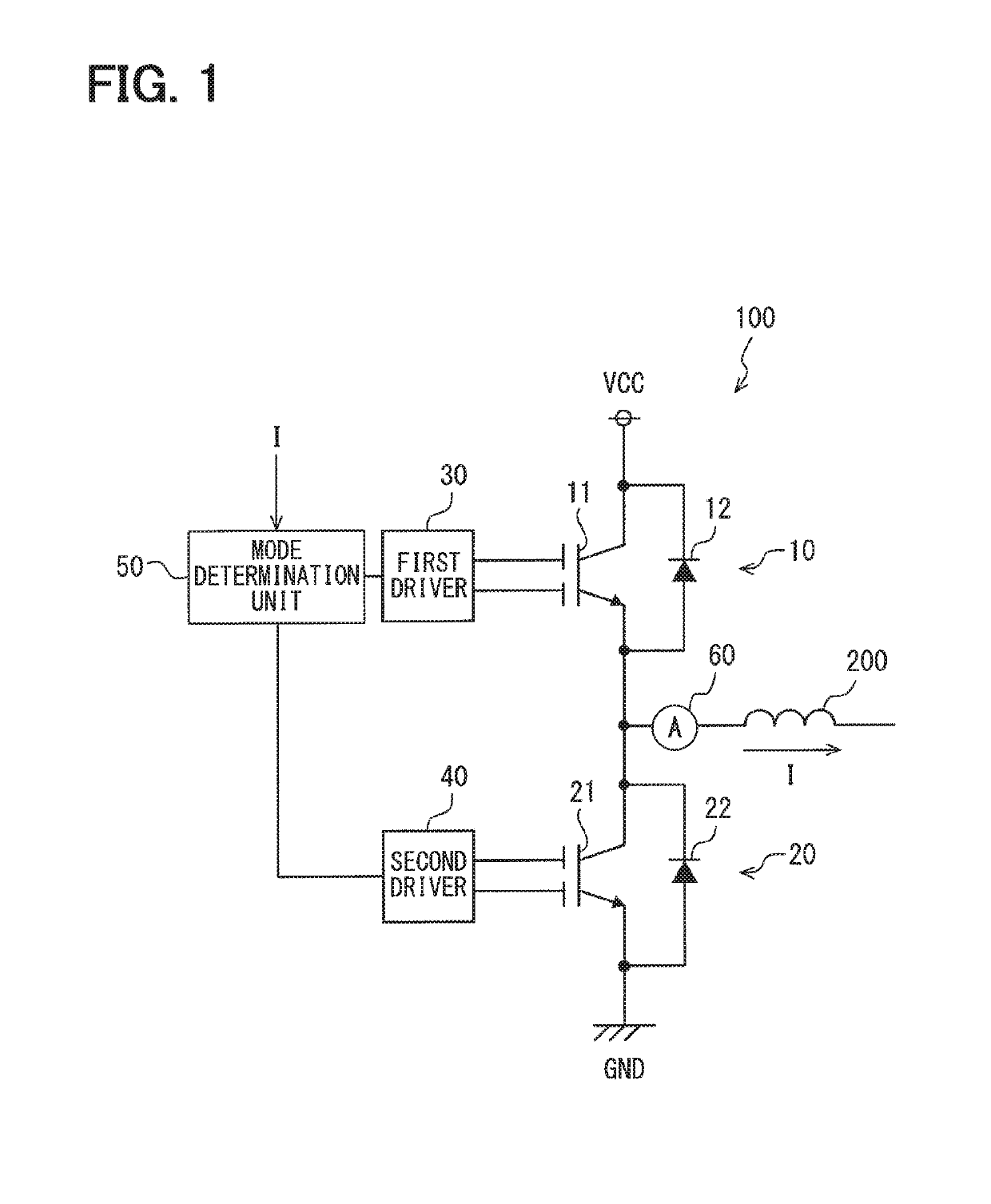
[0024]First, the schematic configuration of a semiconductor device according to the present embodiment will be described with reference to FIG. 1.

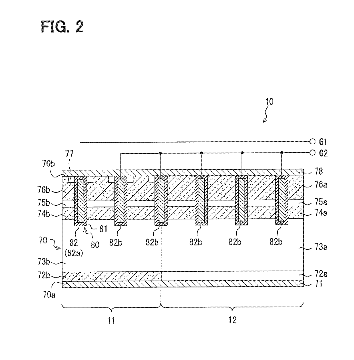
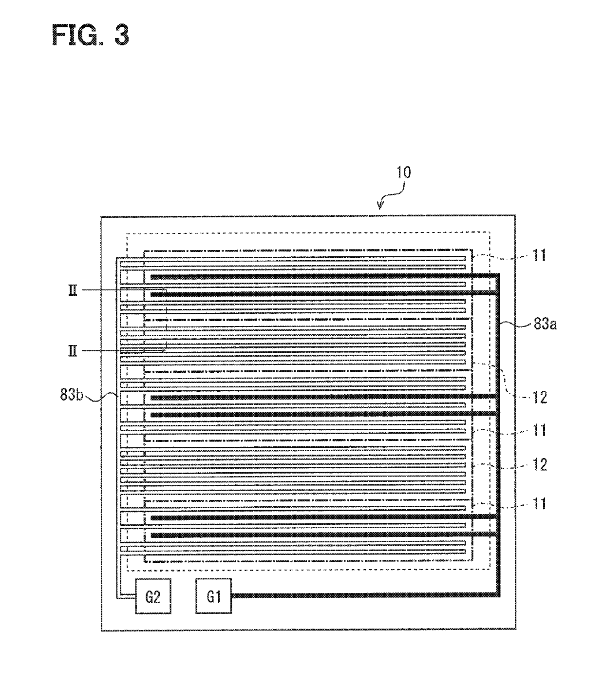
[0025]In the present embodiment, a reverse conducting insulated-gate bipolar transistor (RC-IGBT), having a diode device and an insulated-gate bipolar transistor (IGBT) device on the same semiconductor substrate, will be described.

[0026]The RC-IGBT is applied to an inverter, which is a semiconductor device.

[0027]As shown in FIG. 1, the inverter 100 includes two reverse conducting insulated-gate bipolar transistors 10 and 20, drivers 30 and 40 for applying gate voltage to gate electrodes of the reverse conducting insulated-gate bipolar transistors 10 and 20, respectively, and a mode determination unit 50 that determines the driving state of each of the reverse conducting insulated-gate bipolar transistors 10 and 20.

[0028]As shown in FIG. 1, the inverter 100 is configured to have the two reverse conducting insulated-g...


PUM


Abstract

A semiconductor device includes: reverse conducting switching elements-in each of which a diode element and a switching element are arranged in parallel on a single semiconductor substrate; a driver applying a gate voltage to a plurality of gate electrodes in the reverse conducting switching elements; and a mode determination unit determining whether a forward conduction mode in which a current mainly flows through the switching element or a reverse conduction mode in which the current flows through the diode element is being operated.

Description

CROSS REFERENCE TO RELATED APPLICATION[0001]This application is a U.S. national stage application of International Application No. PCT / JP2016 / 087505 filed on Dec. 16, 2016 and is based on Japanese Patent Application No. 2016-13713 filed on Jan. 27, 2016, the disclosures of which are incorporated herein by reference.TECHNICAL FIELD[0002]The present disclosure relates to a semiconductor device equipped with a switching device and a reverse conducting diode.BACKGROUND[0003]As described in Patent Literature 1, a semiconductor device having a reverse conducting insulated-gate bipolar transistor (RC-IGBT) is known. In the semiconductor device, a negative voltage is applied to an insulated trench gate electrode when an IGBT device region is switched off and circulating current flows to a diode device region.[0004]The semiconductor device allegedly allows holes flowing out from an anode region to be readily injected to a drift layer along the insulated trench gate electrode, whereby the for...

Claims


Application Information

Patent Timeline
Patent Type & Authority Patents(United States)
IPC IPC(8): H01L29/00H01L29/78H01L27/06H01L29/861H01L29/868H01L29/739H01L21/8234H01L27/088H01L27/07H02M7/00H02M1/08H01L29/87H02M7/538H01L29/40
CPCH01L27/088H01L29/868H01L29/78H01L21/823418H02M7/003H01L29/739H02M1/08H01L29/861H01L29/87H01L27/0727H01L27/06H01L29/407H02M7/538H01L29/7397H01L29/0834H01L29/4238H01L29/0696H01L29/083H01L29/7805H01L29/1095H01L29/0623H01L29/7802
Inventor KAKIMOTO, NORIYUKI
Owner DENSO CORP
Why Eureka
Try Eureka