
Semiconductor transistor having superlattice structures

a semiconductor and superlattice technology, applied in the field of transistors, can solve the problems of low forward power loss, marked deterioration of switching behavior, low forward resistance, etc., and achieve the effect of reducing the pitch measurement of the transistor, increasing the channel width per surface area, and increasing the current carrying capacity of the transistor

Active Publication Date: 2019-10-29
ROBERT BOSCH GMBH
View PDF17 Cites 0 Cited by
  • Summary
  • Abstract
  • Description
  • Claims
  • Application Information

AI Technical Summary

Benefits of technology

The present invention is about a transistor structure that has an increased channel width per surface area and higher switching rates compared to conventionally designed transistors. This is achieved by an interconnection of shielding areas, which form a larger contact surface area with lower costs, and higher switching rates. The shielding areas can be embedded directly below the trenches or formed in a regular pattern to improve the stability and operation of the transistor. The interconnection of shielding areas and their joint guidance to terminals guides more than two shielding areas, which significantly reduces the pitch measure of the transistor and reduces the need for high-energy implantation. The transistor structure should have a simplified production process and improve reproducibility while reducing adjustment requirements.

Problems solved by technology

Frequently, trench MOSFETs are used for this purpose, which typically have low forward resistances and therefore low forward power losses.
In trench MOSFETs it is necessary to ensure that the electric field intensity on the gate oxide remains within certain limits since otherwise undesired leakage currents or even the destruction of the gate oxide result.
This connection is necessary for components based on silicon carbide (SiC) since otherwise, due to the minority carrier concentration being lower in comparison to silicon (Si) by orders of magnitude, a recharging of such p-type areas following their depletion takes very long and thus the switching behavior is markedly deteriorated.
This reduces the pitch measure of the transistor accordingly.

Method used


Image

  • Semiconductor transistor having superlattice structures
  • Semiconductor transistor having superlattice structures
  • Semiconductor transistor having superlattice structures

Examples


Embodiment Construction

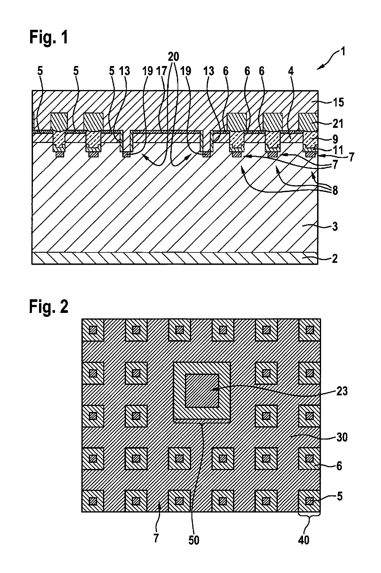
[0025]FIG. 1 shows a transistor 1 according to the present invention, by way of example a trench MOSFET transistor 1, as a lateral view according to a first exemplary embodiment. Transistor 1 shows a layer sequence of a semiconductor material, preferably of silicon carbide (SiC). The lowest layer is formed by a substrate 2 of a first doping type, which typically functions as a drain terminal (metallic contact not drawn). It is followed by an epitaxy layer 3 of the first doping type and a channel layer 4, situated above this epitaxy layer 3, of a second doping type that differs from the first doping type. Furthermore, a plurality of trenches 8 is inserted through channel layer 4 into epitaxy layer 3. In these trenches 8 there is a gate electrode 9, which may be contacted separately. Gate electrode 9 is covered by a gate insulator (not drawn), which electrically insulates gate electrode 9 from the surroundings. An oxide is typically used as gate insulator. Typically, polysilicon is us...


PUM


Abstract

A transistor, including a substrate of a first doping type; an epitaxy layer of the first doping type above the substrate; a channel layer of a second doping type, differing from the first doping type, above the epitaxy layer; a plurality of trenches in the channel layer, which have a gate electrode situated below the trenches and are bordered by a source terminal of the first doping type above the channel layer; a plurality of shielding areas of the second doping type, which are situated below the gate electrode. The shielding areas are guided below the trenches together in a interconnection of shielding areas, and several shielding areas are jointly guided to terminals for contacting the shielding areas.

Description

FIELD[0001]The present invention relates to a transistor, which has a plurality of trenches, in which the gate electrode is situated, and which has interconnected shielding areas to prevent high electric fields.BACKGROUND INFORMATION[0002]Conventional power transistors are produced by connecting individual cells in parallel in the cell field. These individual cells are all identical in order to ensure reliable parallel operation. Currently, partially modified cell structures are used only in the edge area of the transistor, that is, between the cell field and the edge structure or between the cell field and the gate terminal / gate runner. The number of conductive individual cells for a power transistor is currently several thousand.[0003]Frequently, trench MOSFETs are used for this purpose, which typically have low forward resistances and therefore low forward power losses. Trench MOSFETs have a gate electrode within the trenches, which is insulated from the surroundings by a gate in...

Claims


Application Information

Patent Timeline
Patent Type & Authority Patents(United States)
IPC IPC(8): H01L21/02H01L29/78H01L29/423H01L29/06
CPCH01L21/02507H01L29/4236H01L29/0696H01L29/0623H01L29/7813H01L29/7805H01L29/42368
Inventor BANZHAF, CHRISTIAN TOBIASRAMBACH, MARTINGRIEB, MICHAELJACKE, THOMAS
Owner ROBERT BOSCH GMBH
Learn More