Mask blank with resist film and method for manufacturing the same and method for manufacturing transfer mask

a technology of resist film and mask, which is applied in the direction of microlithography exposure apparatus, photomechanical equipment, instruments, etc., can solve the problems of adversely affecting the formation of resist patterns, and achieve the effect of good resist patterns and high degree of freedom in design

Active Publication Date: 2020-03-03
HOYA CORP
View PDF19 Cites 0 Cited by
  • Summary
  • Abstract
  • Description
  • Claims
  • Application Information

AI Technical Summary

Benefits of technology

[0050]According to the present invention, it is possible to provide a technique capable of forming a good resist pattern while maintaining a high degree of freedom in designing the mask blank.

Problems solved by technology

Another reason why the thinning or undercut occurs is a case where a thin film provided under the resist film adversely affects the formation of the resist pattern.

Method used


Image

  • Mask blank with resist film and method for manufacturing the same and method for manufacturing transfer mask
  • Mask blank with resist film and method for manufacturing the same and method for manufacturing transfer mask
  • Mask blank with resist film and method for manufacturing the same and method for manufacturing transfer mask

Examples


example 1

(Preparation of a Sample)

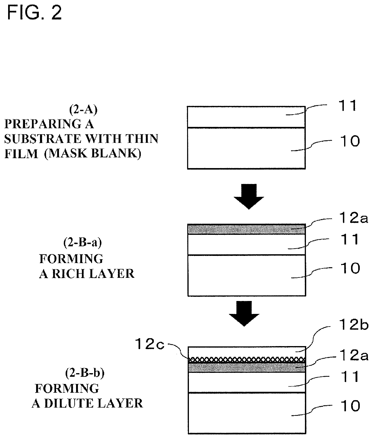
2-A) Preparing a Substrate with Thin Film (Mask Blank 5)

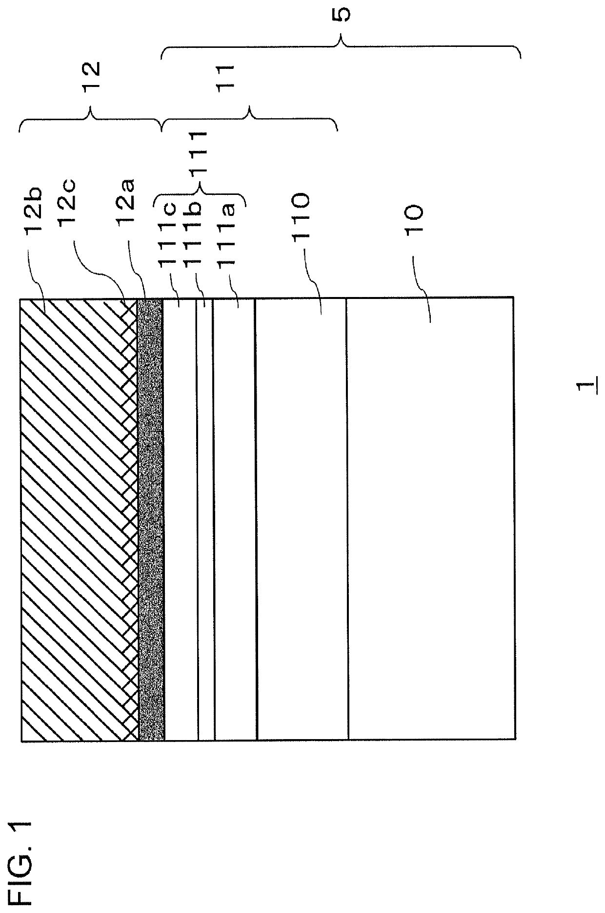
[0162]A light-transmitting substrate 10 (hereinafter also referred to as light-transmitting substrate 10) made of synthetic quartz glass having a main surface dimension of about 152 mm×about 152 mm and a thickness of about 6.25 mm was prepared.

[0163]First, the light semi-transmitting film 110 was formed on the light-transmitting substrate 10.

[0164]A single wafer type sputtering apparatus was used, and a mixed target (mol % ratio of Mo:Si=10:90) of molybdenum (Mo) and silicon (Si) was used as a sputtering target, and a mixed gas of argon (Ar), nitrogen (N2), and helium (He) (flow ratio Ar:N2:He=5:49:46, pressure=0.3 Pa) was used as a sputtering gas, to thereby form MoSiN film (underlayer) on the substrate 10 made of synthetic quartz glass, with a film thickness of 69 nm, by reactive sputtering (DC sputtering: DC power 3.0 kW).

[0165]Subsequently, heat treatment was applied to the substrate 10 on which the...

example 2

[0181]In this example, a sample was prepared in the same manner as in example 1, except that propylene glycol monomethyl ether acetate (PGMEA) was used as the developing solution in the developing step.

(Evaluation)

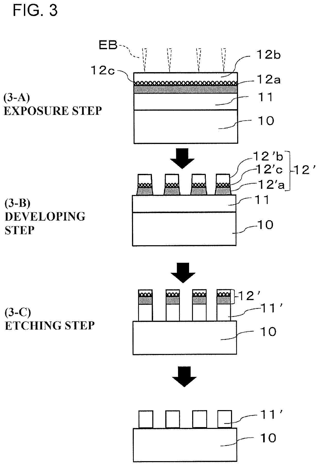
[0182]In this example, the sectional shape of the resist pattern with a half pitch of 200 nm was observed by SEM and its shape was evaluated. FIG. 6 is an SEM image thereof. Referring to FIG. 6, it was found that in this example, the pattern shape can be formed so as to be slightly spread toward the thin film 11 side. Even in the case of this example, collapse never occurred even with a pattern in which the line width was 60 nm or less.

example 3

[0187]In this example, a sample was prepared in the same manner as in example 1, except that the step of forming a rich layer was performed as follows.

[0188]Bis (p-toluenesulfonyl) diazomethane (photoacid generator A′) (WPAG-199 manufactured by Wako Pure Chemical Industries, Ltd.) having a melting point of 122° C. was adjusted into a 5 mass % ethyl acetate solution, and the main surface of the thin film 11 was coated with this solution by a spin coating method, and then baked at 190° C. for 60 seconds, to form the rich layer 12a of 5 nm. Subsequently, the same dilute layer 12b as that of example 1 was formed with a thickness of 100 nm.

(Measurement)

[0189]Distribution of the photoacid generator A′, photoacid generator B and polymer in the depth direction in the mask blank with resist film 1 was confirmed by TOF-SIMS. FIG. 9 shows the results. As shown in FIG. 9, when viewed from the outermost surface of the resist film 12 in the depth direction, a region in which the photoacid generat...


PUM

PropertyMeasurementUnit
degree of freedomaaaaaaaaaa
thicknessaaaaaaaaaa
thicknessaaaaaaaaaa

Abstract

A mask blank with resist film, including a substrate having a thin film; and a negative resist film formed on a main surface of the thin film, wherein in the resist film, a photoacid generator-rich region in which concentration of a photoacid generator is high compared to other region of the resist film, is formed at a portion where the resist film is in contact with the thin film.

Description

TECHNICAL FIELD[0001]The present invention relates to a mask blank with resist film and a method for manufacturing the same and a method for manufacturing a transfer mask.DESCRIPTION OF RELATED ART[0002]A technique of forming a resist film using a negative chemically amplified resist and forming a resist pattern from the resist film is attracting attention because a fine pattern can be formed.[0003]A mechanism of the negative chemically amplified resist is briefly described as follows. First, a photo acid generator (Photo Acid Generator: PAG) is contained in the resist solution. At the same time, a compound capable of causing photocrosslinking or photopolymerization reaction is contained therein. Exposure is performed after applying a resist solution, baking the same, and forming a film. Acid is generated due to a photoacid generator at a place where exposure is performed. The photocrosslinking and the photopolymerization reaction are advanced or promoted by this acid. In this manne...

Claims


Application Information

Patent Timeline
Patent Type & Authority Patents(United States)
IPC IPC(8): G03F1/20G03F7/20G03F7/004G03F7/038G03F1/00G03F7/32G03F7/095G03F7/11
CPCG03F7/32G03F7/11G03F7/2037G03F7/0046G03F1/20G03F1/00G03F7/0045G03F7/0382G03F7/325G03F7/322G03F7/095G03F1/50G03F7/004G03F7/038
Inventor FUKUI, TORU
Owner HOYA CORP
Why Eureka
Try Eureka