Plasma processing apparatus and plasma processing method

a plasma processing and plasma technology, applied in the field of plasma processing apparatus and plasma processing method, can solve the problem that the reflected wave cannot be suppressed, and achieve the effect of improving uniformity in plasma processing, high plasma density, and easy absorbing

Active Publication Date: 2020-06-02
TOKYO ELECTRON LTD
View PDF16 Cites 15 Cited by
  • Summary
  • Abstract
  • Description
  • Claims
  • Application Information

AI Technical Summary

Benefits of technology

[0018]According to the present disclosure, in a plasma processing apparatus using microwaves and plasma processing method using microwaves, uniformity in plasma processing can be improved since the microwaves can be maintained at a frequency which allows the microwaves to be easily absorbed to the plasma and plasma having a uniform and high plasma density can be stably generated within the processing vessel.

Problems solved by technology

However, in Patent Document 1, there is a problem in that since it is difficult to attain matching in the entire band as the frequency band is made broader, reflected waves cannot be suppressed.

Method used


Image

  • Plasma processing apparatus and plasma processing method
  • Plasma processing apparatus and plasma processing method
  • Plasma processing apparatus and plasma processing method

Examples


Embodiment Construction

[0024]Hereinafter, exemplary embodiments of the present disclosure will be described with reference to the accompanying drawings.

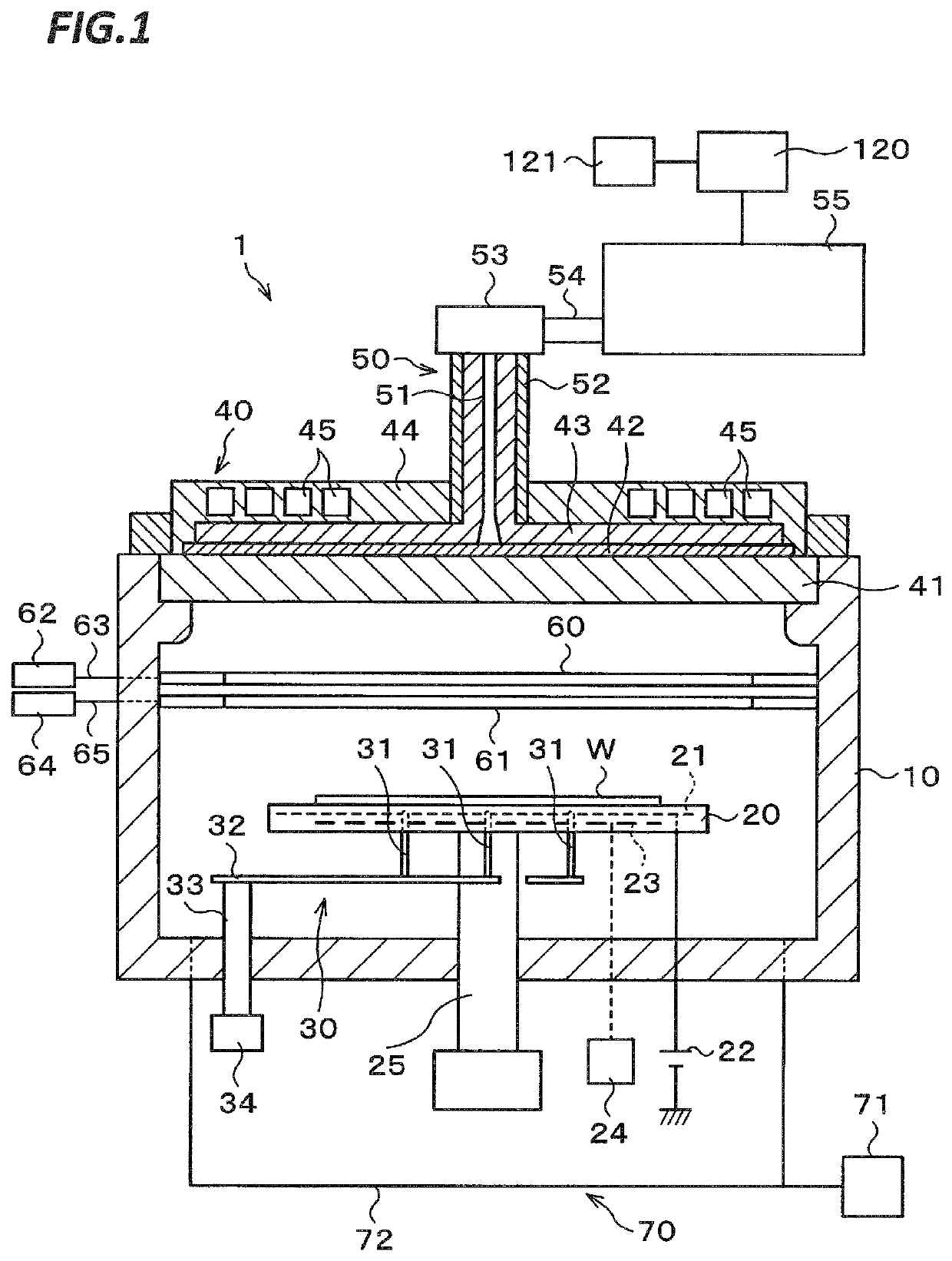
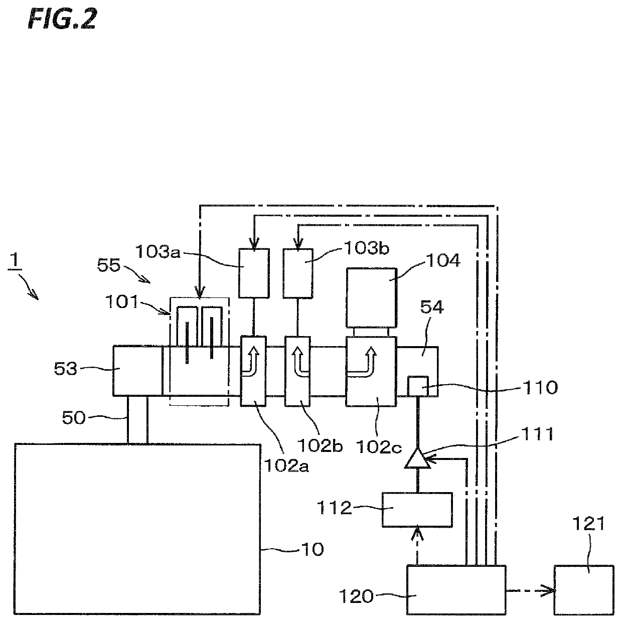
[0025]FIG. 1 is a vertical sectional view illustrating a schematic configuration of a plasma processing apparatus 1 according to an exemplary embodiment of the present disclosure. The plasma processing apparatus 1 is a film forming device that includes a plasma generation mechanism that performs a plasma chemical vapor deposition (CVD) processing on a front surface (top surface) of a wafer W as a processing target object. The present disclosure is not limited to the exemplary embodiments to be described below.

[0026]The plasma processing apparatus 1 includes a processing vessel 10 as illustrated in FIG. 1. The processing vessel 10 has a substantially cylindrical shape having an opened ceiling, and a radial line slot antenna 40 is disposed in the opening of the ceiling. Further, a wafer W carry-in port (not illustrated) is formed in a lateral side of the pro...


PUM

PropertyMeasurementUnit
frequencyaaaaaaaaaa
frequencyaaaaaaaaaa
frequencyaaaaaaaaaa

Abstract

A plasma processing apparatus includes a microwave generation unit configured to generate a microwave, a processing vessel configured to introduce the microwave thereinto, and a gas supply mechanism configured to supply a gas into the processing vessel, plasma being generated within the processing vessel so that a plasma processing is performed on a processing target object. The microwave generation unit includes an oscillation circuit configured to oscillate the microwave, a pulse generation circuit configured to oscillate a control wave having a predetermined frequency bandwidth at a predetermined cycle, and a frequency modulation circuit configured to modulate a frequency of the microwave to a modulated wave having the predetermined frequency bandwidth by the control wave and output the modulated wave, and the frequency modulation circuit alternately and repeatedly outputs the modulated wave and a non-modulated microwave at the predetermined cycle.

Description

CROSS REFERENCE TO RELATED APPLICATIONS[0001]This application is a 35 U.S.C. 371 National Phase Entry Application from PCT / JP2015 / 084040, filed Dec. 3, 2015, which claims priority from Japanese Patent Application No. 2014-263547, filed on Dec. 25, 2014, all of which are incorporated herein by reference.[0002]The present disclosure relates to a plasma processing apparatus configured to excite plasma using microwaves and a plasma processing method.BACKGROUND[0003]A semiconductor element, an organic EL element, or the like is manufactured by performing a processing such as, for example, etching, CVD, or sputtering, on a processing target substrate. In the related art, a plasma processing apparatus using a radial line slot antenna has been known as a plasma processing apparatus that performs a predetermined plasma processing on a processing target object such as, for example, a semiconductor wafer. The radial line slot antenna is disposed on the top of a dielectric window disposed in an...

Claims


Application Information

Patent Timeline
Patent Type & Authority Patents(United States)
IPC IPC(8): H01J37/32C23C14/22H01L21/3065C23C16/511H05H1/46
CPCC23C16/511H01J37/32311H01J37/32192H05H1/46H01L21/3065C23C14/22H01J37/32256H01J37/32275
Inventor KUBOTA, SHINJI
Owner TOKYO ELECTRON LTD
Why Eureka
Try Eureka