Cooled electronics package with stacked power electronics components

a technology of power electronics components and electronics packages, applied in the field of electronics packages, can solve the problems of difficult packaging of power semiconductor chips very dense together, limited switching speed of power semiconductors, and parasitic inductance problems

Active Publication Date: 2020-06-30
ABB (SCHWEIZ) AG
View PDF14 Cites 0 Cited by
  • Summary
  • Abstract
  • Description
  • Claims
  • Application Information

AI Technical Summary

Benefits of technology

[0008]It is an objective of the invention to provide an electronics package with densely packed power electronics components such as semiconductor chips, which is effectively cooled without degrading the electrical performance.
[0016]In other words, the power electronics components may be stacked in the electronics package. For example, two power electronics components may be stacked with respect to each other in the same direction, in which the layers of the electronics package are stacked. Through internally stacking the power electronics components, a high density of active and passive components may be achieved, while the volume of the electronics package is only marginally increased compared to an electronics module without stacked power electronics components. Reducing the distance between power electronics components and connections may result in a low parasitic inductance.
[0019]Furthermore, with the integrated cooling channel, it is possible to eliminate the need for a directly attached, not integrated primary heat sink. Without the primary heat sink, there is no capacitive coupling between the primary heat sink and the electronics package, no need for thermal interface materials and a mechanical fixation to the electronics package. The overall weight of the electronics package may be reduced.
[0023]Furthermore, at least parts of the cooling channel, which extends in a direction substantially parallel to the different layers of the electronics package, may be provided in a part, which may be easy to manufacture with an internal channel. For example, the isolation element may be made of polymer. The cooling channel may be provided in the isolation element before the isolation element is integrated into the support layer.
[0038]According to an embodiment of the invention, the electronics package further comprises two outer layers providing contact areas on both sides of the electronics package. In such a way, several equally designed power electronics packages may be easily stacked and electrically interconnected.
[0043]According to an embodiment of the invention, a first switch chip and a first diode chip electrically connected in parallel are bonded to two opposite sides of a first electrically conducting component of the support layer, which first component is separated from a second electrically conducting component of the support layer by an isolation element, wherein a second switch chip and a second diode chip electrically connected in parallel are bonded to two opposite sides of the second electrically conducting component, and wherein the cooling channel runs through the first component, the isolation element and the second component. This arrangement provides the possibility to stack a switch chip and a diode chip. This may provide a more even temperature distribution inside the electronics package.

Problems solved by technology

The switching speed of power semiconductors is limited by parasitic inductances and capacitances of the electronics package carrying the power semiconductors.
With higher power and higher switching frequencies, for example achievable with wide bandgap semiconductors, the parasitic inductance problems may become worse.
However, packaging the power semiconductor chips very dense together may be challenging in the view of cooling the power semiconductors and a thermal management of the electronics package.
Placing chips closer together may reduce the parasitic problem but the semiconductor chips as heat sources are more proximate to one another which may result in poor thermal spreading and hot spots.
While the global temperature may not be excessive, the local hot spot temperature at a semiconductor chip may prohibit an efficient operation and may reduce the lifetime of the semiconductor chip.
However, this only allows a one-sided cooling and may prevent chip stacking within the electronics package.

Method used


Image

  • Cooled electronics package with stacked power electronics components
  • Cooled electronics package with stacked power electronics components

Examples


Embodiment Construction

[0008]It is an objective of the invention to provide an electronics package with densely packed power electronics components such as semiconductor chips, which is effectively cooled without degrading the electrical performance.

[0009]This objective is achieved by the subject-matter of the independent claims. Further exemplary embodiments are evident from the dependent claims and the following description.

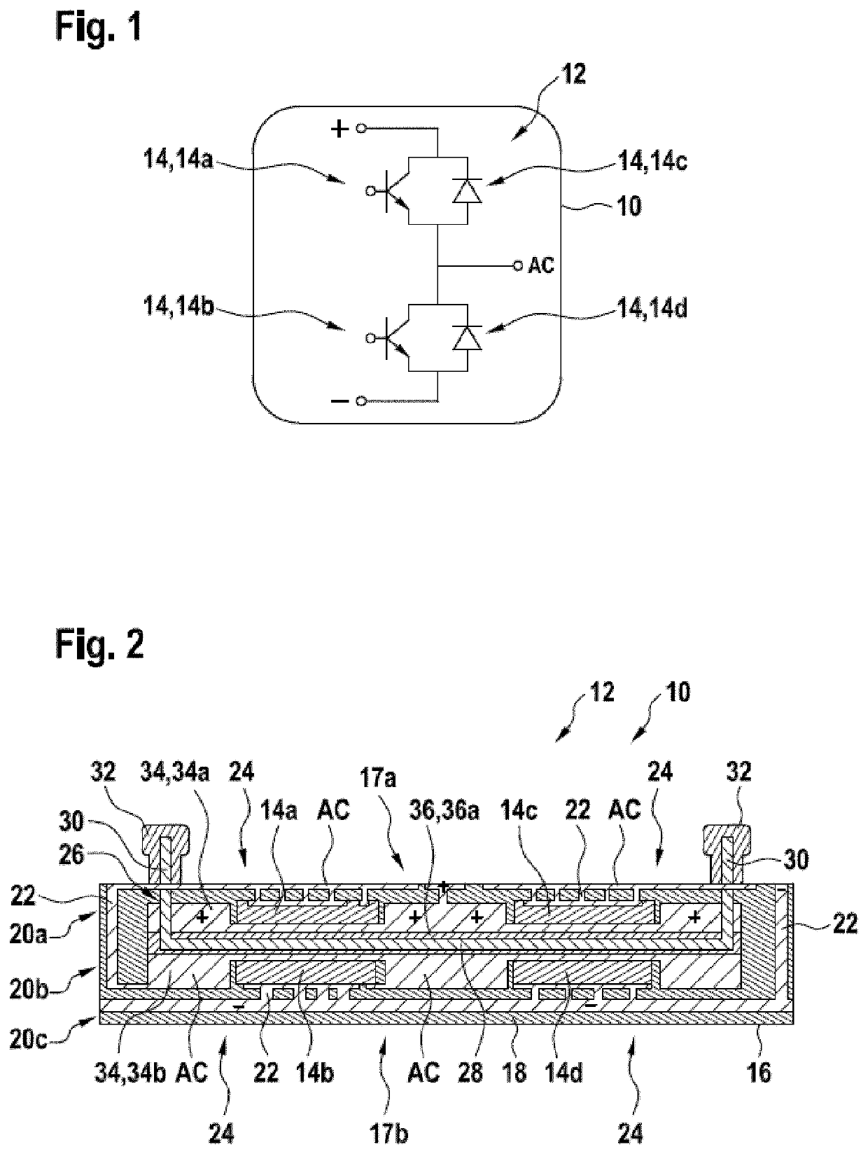
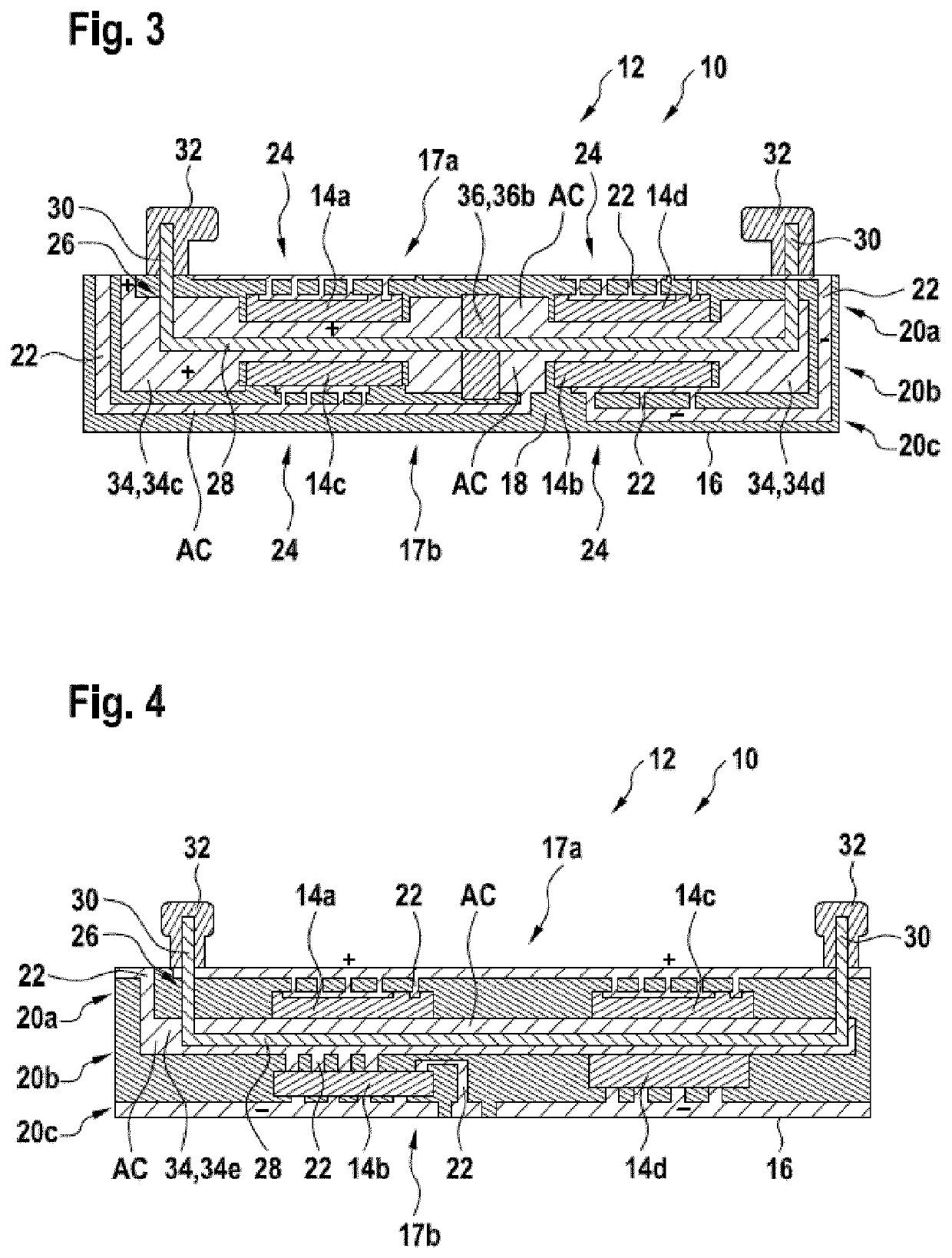
[0010]The invention relates to an electronics package, which may be an assembly comprising power electronics components, such as semiconductor chips, and electrical conductors which are mechanically and electrically interconnected. The electrical conductors may be provided in several layers, which are laminated together with isolation material, such as prepreg material. The power electronics components may be provided inside the electronics package and / or may be arranged in several layers. In such a way, the electronics package may be seen as a multi-layer circuit board.

[0011]The ele...


PUM


Abstract

An electronics package includes an electrically conducting support layer; at least one electrically conducting outer layer; at least two power electronics components arranged on different sides of the support layer and electrically interconnected with the support layer and with the at least one outer layer; and isolation material, in which the support layer and the at least two power electronics components are embedded, the support layer and the at least one outer layer are laminated together with the isolation material; and a cooling channel for conducting a cooling fluid through the electronics package, the cooling channel runs between the at least two power electronics components through the support layer.

Description

FIELD OF THE INVENTION[0001]The invention relates to the field of packaging and cooling of power electronics components. In particular, the invention relates to an electronics package.BACKGROUND OF THE INVENTION[0002]The switching speed of power semiconductors is limited by parasitic inductances and capacitances of the electronics package carrying the power semiconductors. One solution for circuit boards to reduce the parasitics is to embed the power semiconductors and their connections within the substrate of the circuit board. This permits to create short, metallic interconnections, which may minimise distortions due to parasitics.[0003]An embedded technology also may provide the opportunity to embed EMI shield(s) with a high level of isolation from inductively and capacitively coupled noise into the circuit board, which may eliminate the need for an additional surface-mounted shield. With higher power and higher switching frequencies, for example achievable with wide bandgap semi...

Claims


Application Information

Patent Timeline
Patent Type & Authority Patents(United States)
IPC IPC(8): H01L23/34H01L25/07H05K1/02H01L23/473H01L23/538H05K1/18
CPCH05K1/0203H01L25/071H01L23/473H05K1/0272H05K2201/10166H05K1/185H01L23/5386H05K2201/064H01L2224/18H01L2924/15153H01L2224/73267
Inventor KEARNEY, DANIELSCHUDERER, JÜRGENKICIN, SLAVODUARTE, LILIANA
Owner ABB (SCHWEIZ) AG
Why Eureka
Try Eureka