Methods of grinding semiconductor nanocrystal polymer composite particles

a technology of composite particles and nanocrystals, which is applied in the direction of luminescent compositions, instruments, chemistry apparatuses and processes, etc., can solve the problems of reduced efficiency of display devices and poor compatibility of resin materials, and achieve the effect of improving the level of light emitting efficiency

Active Publication Date: 2020-10-20
SAMSUNG ELECTRONICS CO LTD
View PDF13 Cites 0 Cited by
  • Summary
  • Abstract
  • Description
  • Claims
  • Application Information

AI Technical Summary

Benefits of technology

[0005]An embodiment is directed to a method of uniformly grinding a semiconductor nanocrystal-polymer composite without any substantial loss of quantum dot efficiency.
[0050]It therefore becomes possible to provide semiconductor-polymer composite particles that may maintain an improved level of light emitting efficiency.

Problems solved by technology

However, such resin materials may often exhibit poor compatibility with an organic ligand compound being present on the surface of the semiconductor nanocrystal.
The poor compatibility may lead to agglomeration of the semiconductor nanocrystals or may cause a loss of the organic ligand on the surface of the semiconductor nanocrystal, and thereby the display device may show reduced efficiency.

Method used


Image

  • Methods of grinding semiconductor nanocrystal polymer composite particles
  • Methods of grinding semiconductor nanocrystal polymer composite particles
  • Methods of grinding semiconductor nanocrystal polymer composite particles

Examples


reference example 1

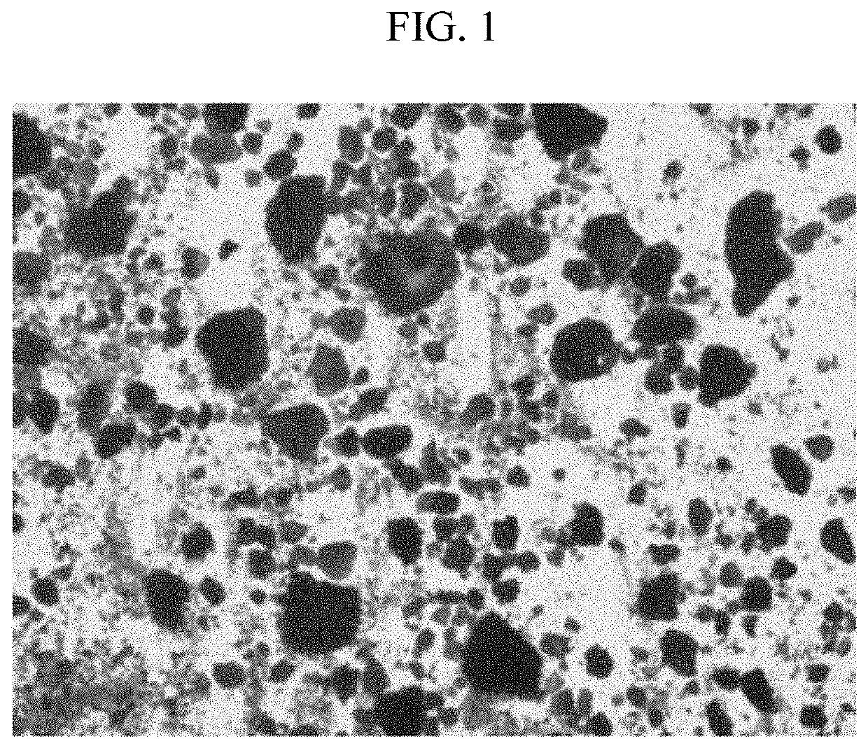
/ SnSeS Semiconductor Nanocrystal-Polymer Composite Particle (Prior to the Low Temperature Grinding)

[0184](1) 0.058 grams (g) of indium acetate, 0.0183 g of zinc acetate, 0.204 g of palmitic acid, and 10 milliliters (mL) of 1-octadecene are placed in a flask, subjected to a vacuum at 120° C. for one hour, and then heated to 280° C. after the atmosphere in the flask is exchanged with N2. After the temperature is stabilized at 280° C., a mixed solution of 0.43 μL of tris(trimethylsilyl)phosphine and 1 mL of trioctylphosphine (“TOP”) is quickly injected and the reaction proceeds for 10 minutes. Then, the mixture is rapidly cooled and acetone is added thereto to produce nanocrystals, which are then separated by centrifugation and dispersed in toluene. The first UV absorption maximum of the prepared InZnP core nanocrystals is 440˜460 nm. 0.056 g of zinc acetate, 0.189 g of oleic acid, and 10 mL of trioctylamine are placed in a flask, subjected to a vacuum at 120° C. for 10 minutes, and th...

example 1

ane as an Inert Organic Solvent

[0187]The semiconductor nanocrystal-polymer composite particle prepared in the Reference Example 1 is subjected to the low temperature grinding using a cryogenic ball milling device (manufactured by JAS (Japan Analytical Industry), JFC-2000). A mixture of 1 g of the InZnP / SnSeS semiconductor nanocrystal-polymer composite particles prepared in the Reference Example 1 and 1 g of hexane is placed in a container with balls for the cryogenic milling. The container is closed, and then a milling rod is connected. The container is immersed and maintained in liquid nitrogen for five minutes. Then, the cryogenic milling is conducted at a frequency of 50 Hertz (Hz) for four cycles. One cycle is five minute milling and a five minute break. After the cryogenic milling, the container is removed from liquid nitrogen and allowed to warm to room temperature. Then, the resulting slurry including hexane and the semiconductor nanocrystal-polymer composite fine particles a...
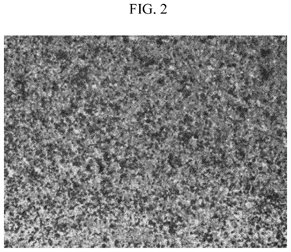
examples 2 to 5

an Inert Organic Solvent

[0188]The ground fine particles of the semiconductor nanocrystal-polymer composite are prepared as according to Example 1, except for changing the amount of hexane and the repetition number of cycles as shown in Table 1.

[0189]An optical microscope image (50×) of the ground find particles obtained in Example 2 is shown in FIG. 2.


PUM

PropertyMeasurementUnit
diameteraaaaaaaaaa
particle sizeaaaaaaaaaa
quantum efficiencyaaaaaaaaaa

Abstract

A method of grinding a semiconductor nanocrystal-polymer composite, the method including obtaining a semiconductor nanocrystal-polymer composite including a semiconductor nanocrystal and a first polymer, contacting the semiconductor nanocrystal-polymer composite with an inert organic solvent; and grinding the semiconductor nanocrystal-polymer composite in the presence of the inert organic solvent to grind the semiconductor nanocrystal-polymer composite.

Description

CROSS-REFERENCE TO RELATED APPLICATION[0001]This application is a continuation-in-part of U.S. patent application Ser. No. 14 / 453,723, filed on Aug. 7, 2017, and which has issued as U.S. Pat. No. 9,701,898, and claims priority to and the benefit of Korean Patent Application No. 10-2013-0094420, filed on Aug. 8, 2013, and all the benefits accruing therefrom under 35 U.S.C. § 119, the contents of which are incorporated herein in their entirety by reference.BACKGROUND1. Field[0002]A process for grinding semiconductor nanocrystal polymer composite particles is disclosed.2. Description of the Related Art[0003]A semiconductor nanocrystal (also known as a quantum dot) is a nano-scale crystalline semiconductor material. The semiconductor nanocrystal has a very small size and a large surface area per unit volume, and may exhibit a quantum confinement effect. As a result of its small size, the semiconductor nanocrystal has different physicochemical characteristics than a bulk material having ...

Claims


Application Information

Patent Timeline
Patent Type & Authority Patents(United States)
IPC IPC(8): C09K11/02G02F1/1335C09K11/59G02F1/361C08L33/04C01B17/20B24B1/00
CPCC08L33/04C09K11/025B24B1/00C09K11/59G02F1/1335G02F1/3615C01B17/20
Inventor LEE, JEONG HEEKANG, HYUN AJANG, EUN JOOLEE, SANG EUIJUN, SHIN AECHO, OULKIM, TAE GONKIM, TAE HYUNG
Owner SAMSUNG ELECTRONICS CO LTD
Why Eureka
Try Eureka