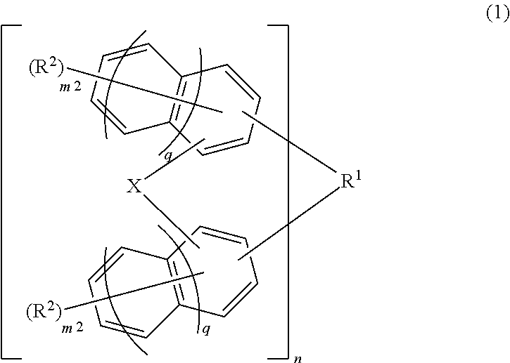
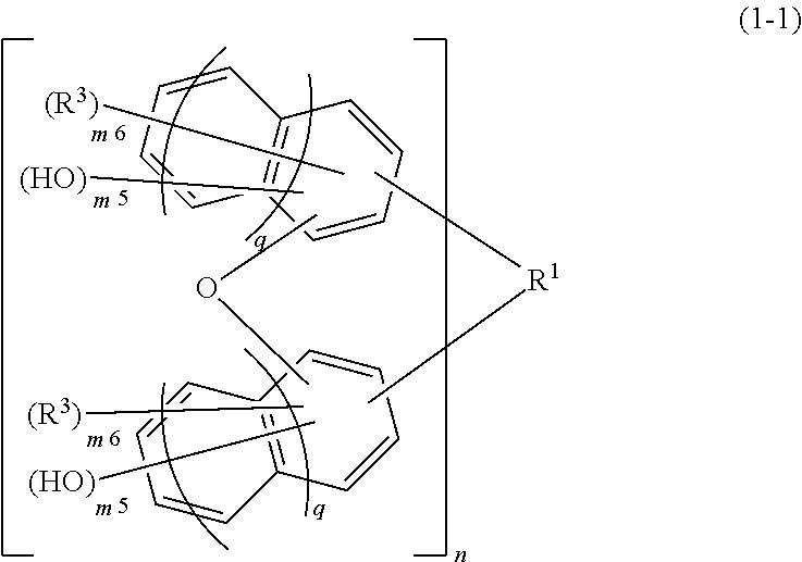
Material for forming underlayer film for lithography, composition for forming underlayer film for lithography, underlayer film for lithography and production method thereof, and resist pattern forming method
a technology of composition and lithography, applied in the direction of photosensitive material processing, photomechanical equipment, instruments, etc., can solve the problem of high solvent solubility and achieve the effect of excellent heat resistance and etching resistan
- Summary
- Abstract
- Description
- Claims
- Application Information
AI Technical Summary
Benefits of technology
Problems solved by technology
Method used
Image


Examples
example 9
[0310]Then, the composition for forming an underlayer film for lithography in Example 1 was coated on a SiO2 substrate having a film thickness of 300 nm, and baked at 240° C. for 60 seconds and further at 400° C. for 120 seconds to thereby form an underlayer film having a film thickness of 85 nm. A resist solution for ArF was coated on the underlayer film, and baked at 130° C. for 60 seconds to thereby form a photoresist layer having a film thickness of 140 nm. Herein, as the resist solution for ArF, one prepared by blending 5 parts by mass of the compound represented by the following formula (5), 1 part by mass of triphenylsulfonium nonafluoromethanesulfonate, 2 parts by mass of tributylamine, and 92 parts by mass of PGMEA was used.
[0311]A compound represented by formula (5) was prepared as follows. That is, 4.15 g of 2-methyl-2-methacryloyloxyadamantane, 3.00 g of methacryloyloxy-γ-butyrolactone, 2.08 g of 3-hydroxy-1-adamantyl methacrylate and 0.38 g of azobisisobutyronitrile wer...
example 10
[0319]The composition for forming an underlayer film for lithography used in Example 1 was coated on a SiO2 substrate having a thickness of 300 nm, and baked at 240° C. for 60 seconds and further at 400° C. for 120 seconds to thereby form an underlayer film having a thickness of 90 nm. A silicon-containing intermediate layer material was coated on the underlayer film, and baked at 200° C. for 60 seconds to thereby form an intermediate layer film having a thickness of 35 nm. Furthermore, the resist solution for ArF was coated on the intermediate layer film, and baked at 130° C. for 60 seconds to thereby form a photoresist layer having a thickness of 150 nm. Herein, as the silicon-containing intermediate layer material, a silicon atom-containing polymer obtained below was used.
[0320]In 200 g of tetrahydrofuran (THF) and 100 g of pure water were dissolved 16.6 g of 3-carboxypropyltrimethoxysilane, 7.9 g of phenyltrimethoxysilane and 14.4 g of 3-hydroxypropyltrimethoxysilane, the liquid...
PUM
| Property | Measurement | Unit |
|---|---|---|
| temperature | aaaaa | aaaaa |
| temperature | aaaaa | aaaaa |
| thickness | aaaaa | aaaaa |
Abstract
Description
Claims
Application Information
 - R&D
- Intellectual Property
- Life Sciences
- Materials
- Tech Scout
- Unparalleled Data Quality
- Higher Quality Content
- 60% Fewer Hallucinations
Browse by: Latest US Patents, China's latest patents, Technical Efficacy Thesaurus, Application Domain, Technology Topic, Popular Technical Reports.
© 2025 PatSnap. All rights reserved.Legal|Privacy policy|Modern Slavery Act Transparency Statement|Sitemap|About US| Contact US: help@patsnap.com