Wireless communication system

a communication system and wireless technology, applied in the direction of low-noise amplifiers, power management, amplifiers with min 3 electrodes or 2 pn junctions, etc., can solve the problems of increased length of wires, reduced gain, and degraded noise characteristics

Inactive Publication Date: 2001-08-23
RENESAS ELECTRONICS CORP
View PDF3 Cites 42 Cited by
  • Summary
  • Abstract
  • Description
  • Claims
  • Application Information

AI Technical Summary

Problems solved by technology

(a) In the case of the conventional signal processing IC having a power source line and a ground line arranged between the edge portion of the semiconductor chip and pads to be connected with wirings, the wirings for connecting the pads and the inner ends of leads become longer by the length over the power source and ground lines, so that the gain is reduced and the noise characteristic is degraded.
(b) In also the case of the conventional signal processing IC in which the power source line or the ground line is arranged between the LNA circuit and the pads, similarly to the foregoing, the length of the wiring is increased more, the gain is reduced and the noise characteristi

Method used


Image

  • Wireless communication system
  • Wireless communication system
  • Wireless communication system

Examples


first embodiment

[0040] (First Embodiment)

[0041] FIGS. 1 to 7 are figures each of which relates to a wireless communication system according to a first embodiment of the present invention. In the first embodiment, an example in which the present invention is applied to a wireless communication system of a TDMA (Time Division Multiple Access) system, e.g., a terminal apparatus of a wireless communication mobile body will hereinbelow be described in detail.

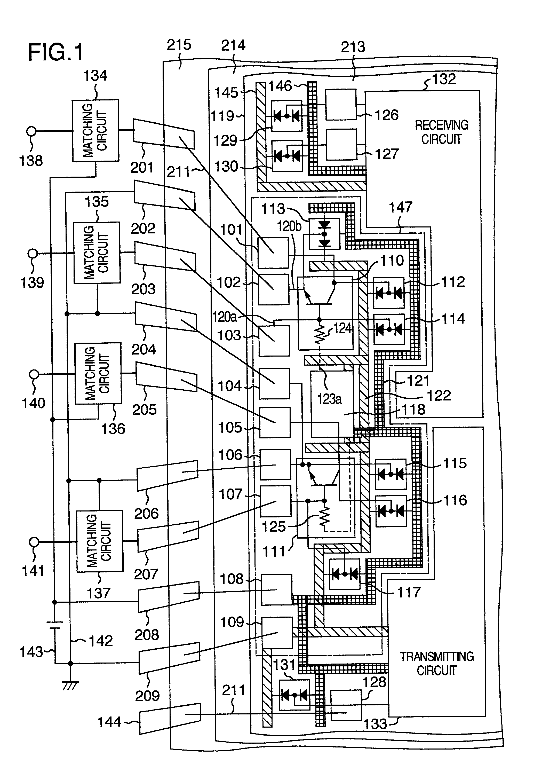
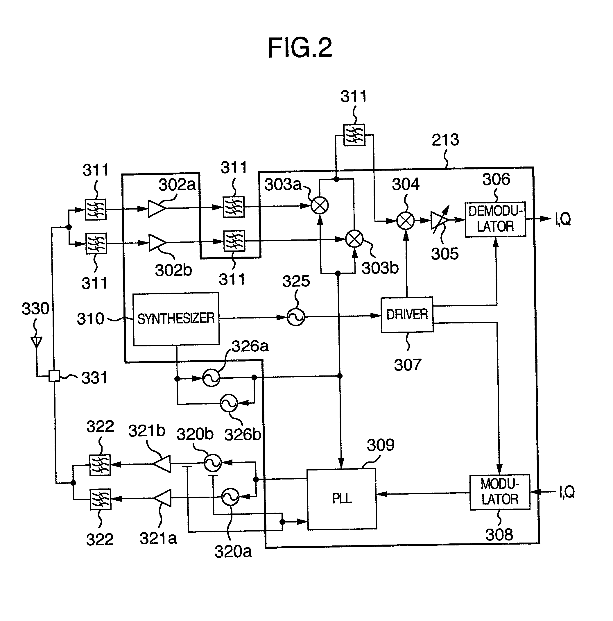
[0042] Now, a configuration of a TDMA dual band wireless communication terminal apparatus will hereinbelow be described with reference to FIG. 2. This terminal apparatus can execute the signal processing for a GSM system of a 900 MHz band and a DCS 1800 system of a 1800 MHz band.

[0043] In a block diagram shown in FIG. 2, a transmitting and receiving circuit electrically connected to an antenna 330 through a transmitting and receiving switching unit 331 are both shown and each of them is connected to a base band signal processing circuit (not shown)....

second embodiment

[0097] (Second Embodiment)

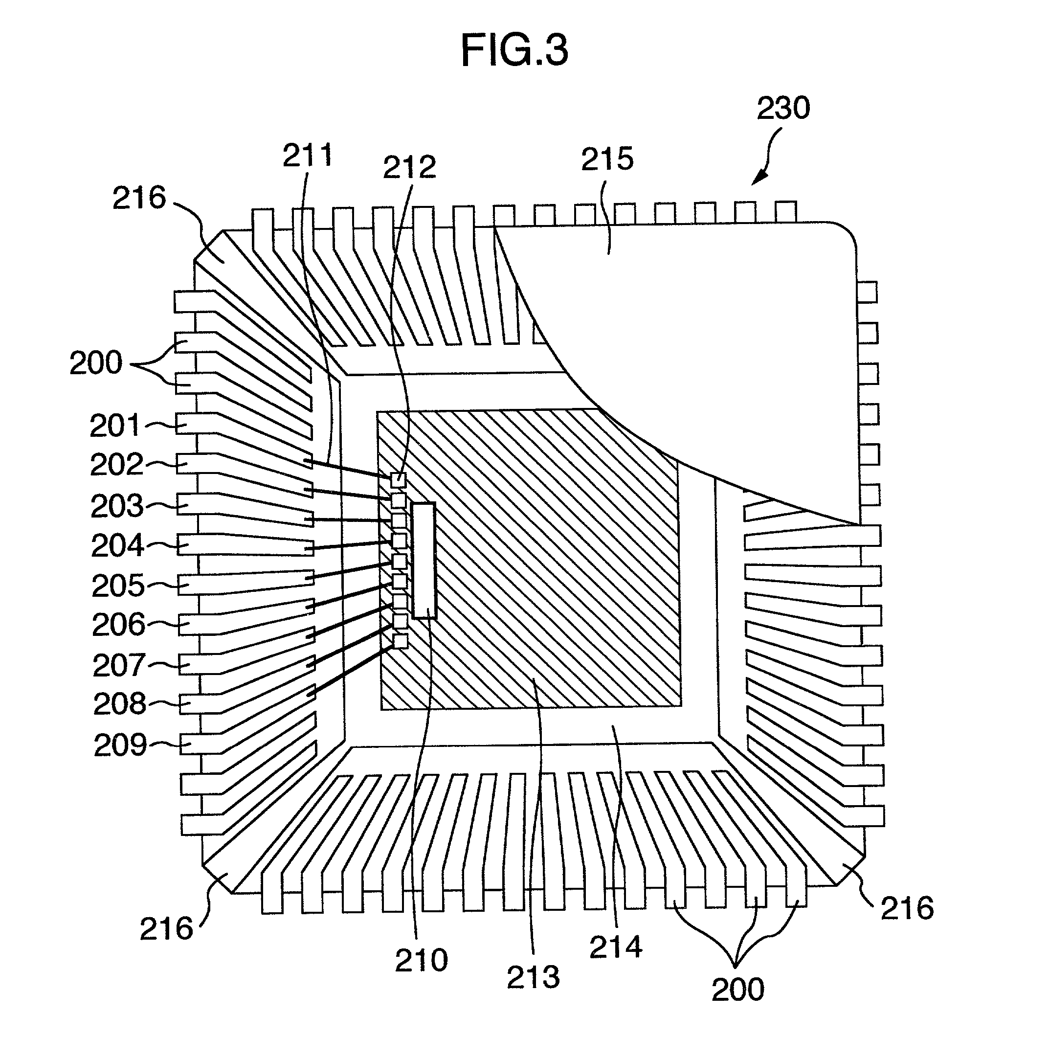
[0098] FIG. 8 is a schematic block diagram, partly in circuit diagram, showing a configuration in part of a semiconductor integrated circuit device, in which the low-noise amplifiers 110 and 111 are both incorporated in a dual band wireless communication system according to a second embodiment of the present invention, and FIG. 9 is a schematic plan view showing the wiring pattern of a bipolar transistor constituting the low-noise amplifier 110 in the IC chip 213 which is incorporated in the wireless communication system of the second embodiment.

[0099] While in the first embodiment shown in FIG. 1, the part in which the bias circuit 118 is provided between the LNA 110 for the low frequency band and the LNA 111 for the high frequency band has the layout in which the peripheral part of the LNA circuit 147 becomes hollow inwardly with respect to the flat surface, the area which becomes hollow inwardly with respect to the flat surface may not be effectively uti...

third embodiment

[0104] (Third Embodiment)

[0105] FIGS. 10 and 11 show a third embodiment of the present invention. FIG. 10 is a schematic cross sectional view showing the construction of a CSP (Chip Size Package) containing a semiconductor integrated circuit device, which is incorporated in the wireless communication system, and FIG. 11 is a block diagram, partly in circuit diagram, showing the layout of a multilayer ceramic substrate and the like in which the CSP containing the semiconductor integrated circuit device is incorporated.

[0106] The CSP has the construction in which solder bumps 601 are respectively provided on the pads (not shown) of the IC chip 213; these solder bumps 601 are respectively bonded to the pads (not shown) on the surface of a multilayer ceramic substrate 603 to be attached thereto; and a filler 602 is led into the space defined between the IC chip 213 and the multilayer ceramic substrate 603 to fix the IC chip 213 to the multilayer ceramic substrate 603. In addition, the r...


PUM


Abstract

A wireless communication system includes: a filter; and a semiconductor chip including a signal processing integrated circuit having an amplifier, wherein a main surface of the semiconductor chip is provided with a plurality of electrode terminals along an edge portion thereof; wherein the amplifier has a transistor including a control electrode, a first electrode through which a signal is outputted, and a second electrode to which a voltage is applied; wherein the control electrode, the first electrode and the second electrode of the transistor are connected to the electrode terminals, respectively; and wherein none of wirings are arranged between the electrode terminals and placements of the control electrode, the first electrode and the second electrode, making space between the electrodes and the electrode terminals narrow.

Description

[0001] 1. Field of the Invention[0002] The present invention relates, in general, to a wireless communication system. More particularly, the invention relates to the technology which is effectively employed to the layout technique of internal circuits of a reception integrated circuit for the wireless communication in which the high frequency characteristics become excellent.[0003] 2. Description of the Related Art[0004] In a signal processing integrated circuit (IC) in a wireless communication system (an terminal apparatus of a wireless communication mobile body; it will hereinafter also be referred to as "a terminal apparatus" for short, when applicable) such as a digital cellular system, a large number of internal circuits are incorporated in a single semiconductor chip.[0005] The signal processing IC for example, is described in an article of "DIGEST OF TECHNICAL PAPERS", ISSC98 / Feb. 5, 1998, pp. 48 to 49, pp. 441 "A SINGLE-CHIP CMOS TRANSCEIVER FOR DCS1800 WIRELESS COMMUNICATIO...

Claims


Application Information

Patent Timeline
IPC IPC(8): H01L23/48H01L21/82H01L27/02H01L29/417H03F3/14H04B1/18H04B1/38H04B1/3822
CPCH01L23/48H01L24/06H01L27/0203H01L29/41708H01L2224/05553H01L2224/05624H01L2224/48247H01L2924/01004H01L2924/01006H01L2924/01013H01L2924/01014H01L2924/01082H01L2924/014H04W52/52H01L2924/00014H01L2924/01005H01L2924/01033H01L2224/32225H01L2224/73204H01L2924/13091H03F3/19H03F3/68H03F2200/294H03F2200/429H03F2200/451H04B1/0075H01L2924/30107H01L2924/00H01L2924/1306H01L2924/1305H01L2924/15787H01L2924/181H01L2224/48465H01L2224/04042H01L2224/05554H01L2224/05093H01L2924/14H01L2224/06H01L2224/16225H01L2924/00012H04B1/18H01L23/4952H01L23/49541H01L23/49575H01L23/66
Inventor TAKIKAWA, KUMIKOTANAKA, SATOSHITASHIRO, YOSHIYASU
Owner RENESAS ELECTRONICS CORP
Why Eureka
Try Eureka