Eureka AIR delivers breakthrough ideas for toughest innovation challenges, trusted by R&D personnel around the world.

Metal wire fuse structure with cavity

Inactive Publication Date: 2001-09-13
INFINEON TECH AG
View PDF0 Cites 2 Cited by
  • Summary
  • Abstract
  • Description
  • Claims
  • Application Information

AI Technical Summary

Problems solved by technology

Both those methods result in large fuse pitches and significant use of chip area.
In cases where the fusible links: are built from the same material as the chip conductors; become thicker; are made of composite layers including layers of refractory metals (tungsten and various silicides); or are comprised of highly reflective metals (copper / aluminum), blowing the fuses with lasers becomes more difficult.
It has been found that the use of a laser beam to set, cut or blow a fuse link may render the area under the fuse link or adjacent fusible links vulnerable to laser-induced damage, mainly due to the absorption of laser energy during the fuse setting operation.
Because of the possibility of laser-induced damage, the areas underlying the fuse links are typically devoid of semiconductor devices (e.g., transistors) and the fuses are spaced far apart in conventional systems.
Even when there are no active devices beneath the fusible link or other closely spaced fusible links, the substrate itself may also experience some degree of laser-induced damage.
Even though infrared lasers are helpful in minimizing laser-induced damage to the underlying substrate, the use of lasers having relatively long wavelengths involves certain undesirable compromises.
By way of example, the relatively long wavelength of the infrared laser forms a relatively large spot on the substrate during the fuse setting operation, which limits how closely the fuse links can be packed next to one another.
If the fuses are placed too closely together for a given laser wavelength, an adjacent fuse link may be inadvertently blown or cut, rendering the IC defective.
However, a shorter wavelength laser substantially increases the likelihood of underlying substrate damage in conventional systems since the silicon substrate absorbs laser energy from shorter wavelength lasers much more readily.
If a shorter wavelength laser is employed to set the fuse links of the conventional system's fuse array 106, excessive substrate damage in area 320 may result, possibly leading to integrated circuit defects and failure.

Method used


Image

  • Metal wire fuse structure with cavity
  • Metal wire fuse structure with cavity
  • Metal wire fuse structure with cavity

Examples


Embodiment Construction

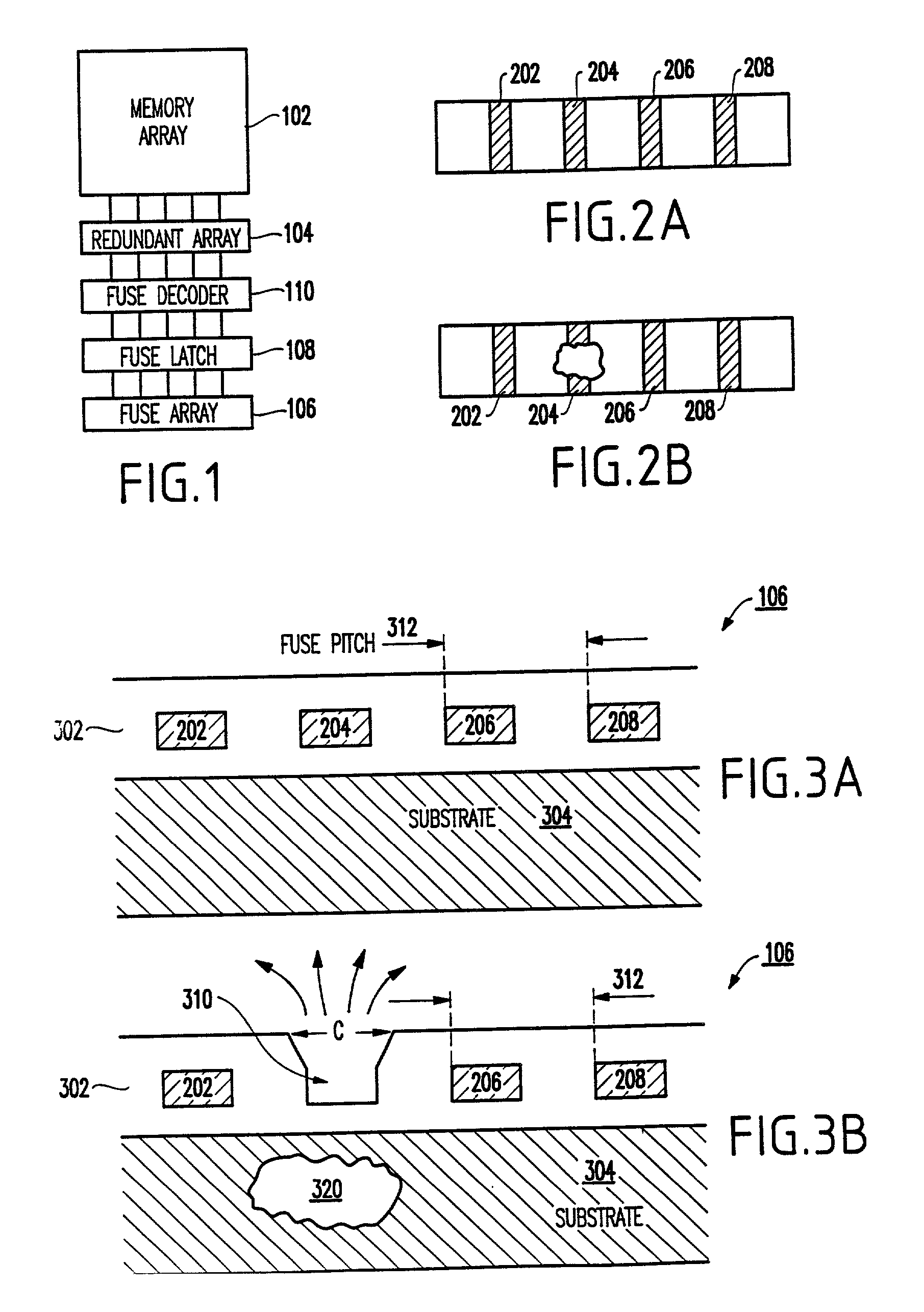
[0032] In order to avoid damage to surrounding structures when a fuse link blows, a cavity may be formed next to the fuse link to absorb some of the energy and the vaporized fuse material expelled during the fuse clearing process. The invention includes a uniquely and conveniently formed and uniquely located cavity which directs the energy and material from the clearing fuse away from structures which might otherwise be damaged.

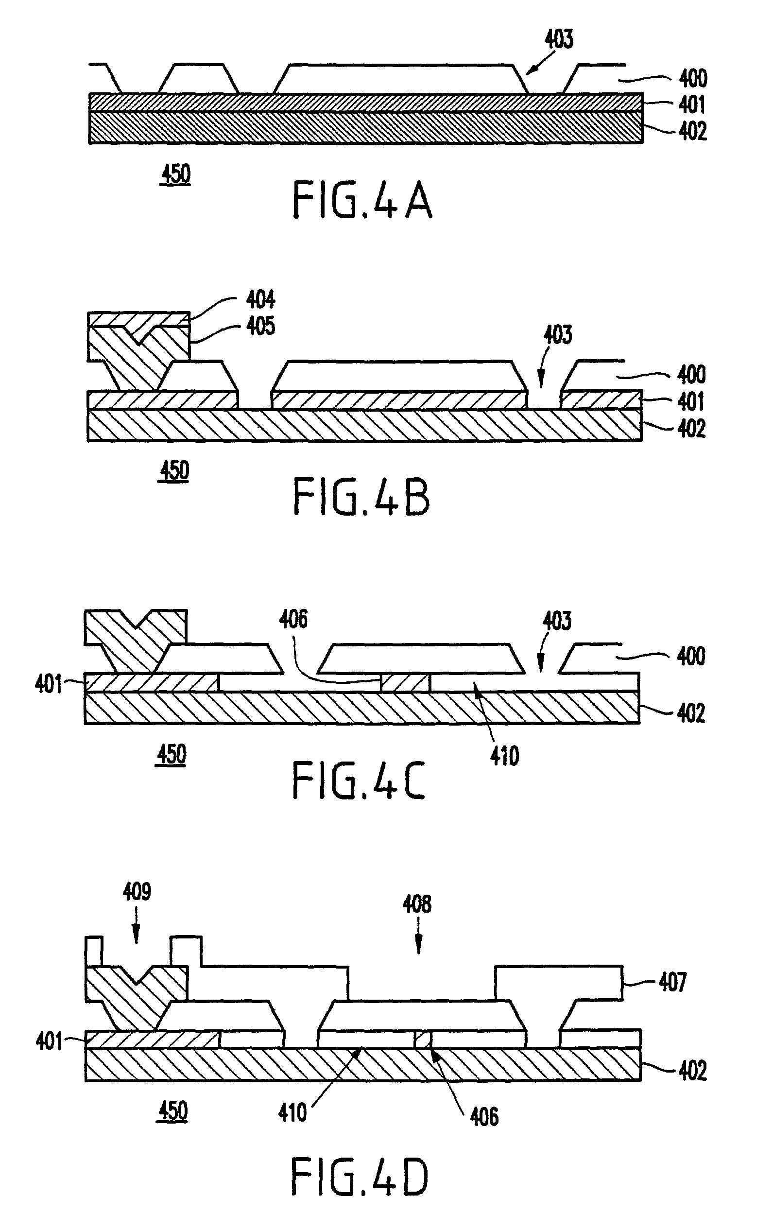
[0033] More specifically, referring to FIGS. 4A-4D, a first embodiment of the inventive fuse structure / process is illustrated. FIG. 4A illustrates a cross section of a metal wire stack (e.g. a first conductive "R1" structure) formed by conventional deposition techniques, photolithography and plasma etching such as sputtering. The wire stack preferably includes a dielectric substrate 450, a first thin conductive (Ti) under layer 402 that is 5 nm-50 nm thick, a second conductive (AlCu alloy) layer 401 that is 10 nm-1000 nm thick. In this structure the AlCu allo...


PUM


Abstract

An integrated circuit has primary devices and redundant devices being selective substituted for the primary devices through at least one fuse. The fuse includes a first layer having at least one fuse link region, a second layer over the first layer and cavities in the second layer above the fuse link region.

Description

[0001] 1. Field of the Invention[0002] The present invention generally relates to the fabrication of integrated circuits. More particularly, the present invention relates to improved techniques for increasing circuit density and / or reducing substrate damage in an integrated circuit employing fusible links.[0003] 2. Description of Related Art[0004] Semiconductor integrated circuits (IC) and their manufacturing techniques are well known. In a typical integrated circuit, a large number of semiconductor devices may be fabricated on a silicon substrate. To achieve the desired functionality, a plurality of conductors are typically provided to couple selected devices together.[0005] In some integrated circuits, conductive links are coupled to fuses, which may be cut or blown after fabrication using lasers or electrical power. In a dynamic random access memory (DRAM) circuit, for example, fuses may be employed during manufacturing to protect some of the transistors' gate stacks from an inad...

Claims


Application Information

Patent Timeline
IPC IPC(8): H01L21/82G11C29/04H01H85/00H01L21/8242H01L23/525H01L27/02H01L27/108
CPCH01L23/5258H01L2924/3011H01L2924/0002H01L2924/00H01L27/02
Inventor BRINTZINGER, AXEL C.KIEWRA, EDWARD W.NARAYAN, CHANDRASEKHARRADENS, CARL J.
Owner INFINEON TECH AG
Why Eureka
Eureka Blog
Learn More