Method of polishing silicon wafer

a technology of silicon wafer and polishing agent, which is applied in the direction of polishing compositions with abrasives, manufacturing tools, lapping machines, etc., can solve the problems of deteriorating the performance of the semiconductor device manufactured from the wafer, increasing the manufacturing cost, and commercially available high-purity silica-containing abrasives

Inactive Publication Date: 2001-11-01
SUMITOMO MITSUBISHI SILICON CORP
View PDF0 Cites 5 Cited by
  • Summary
  • Abstract
  • Description
  • Claims
  • Application Information

AI Technical Summary

Problems solved by technology

Accordingly, when the silicon wafer is polished by such a commercially available alkaline silica-containing abrasive agent in which the metallic impurities are present, among the metallic impurities, metal ions, such as copper ion, nickel ion, chromium ion, iron ion, diffuse in a deep interior of the wafer in the course of polishing step, and cannot be easily removed even at the next cleaning step, thereby deteriorating a performance of the semiconductor device manufactured from the wafer, as is known in the art.
However, a commercially available high-purity silica-containing abrasive agent is so expensive as to increase the manufacturing cost, so that it cannot be employed for the actual production.
Further, even when

Method used


Image

  • Method of polishing silicon wafer

Examples


first embodiment

[0024] First Embodiment

[0025] Hereinafter, a first embodiment of the present invention will be described.

[0026] First, referring to FIG. 2, description will be made as to a polishing apparatus which is used in a method of polishing a silicon wafer according to the first embodiment.

[0027] The polishing apparatus has a rotational disk 1, a wafer holder 2 and an abrasive agent supplying unit 3.

[0028] The rotational disk 1 has a rotational disk supporting body 4, the upper surface thereof being attached with an abrasive pad 5. The rotational supporting disk 1 is rotated by a rotational axis 6 at a predetermined rotational speed.

[0029] The wafer holder 2 holds the wafer 9 on the lower surface thereof by means of vacuum adsorption or the like method, and presses the wafer 9 onto the abrasive pad 5 at a predetermined load while the holder 2 is being rotated by the rotation shaft 7.

[0030] The abrasive agent supplying apparatus 3 supplies an abrasive agent 8 onto the abrasive pad 5 at a pred...

second embodiment

[0048] Second Embodiment

[0049] Hereinafter, a second embodiment of the present invention will be described.

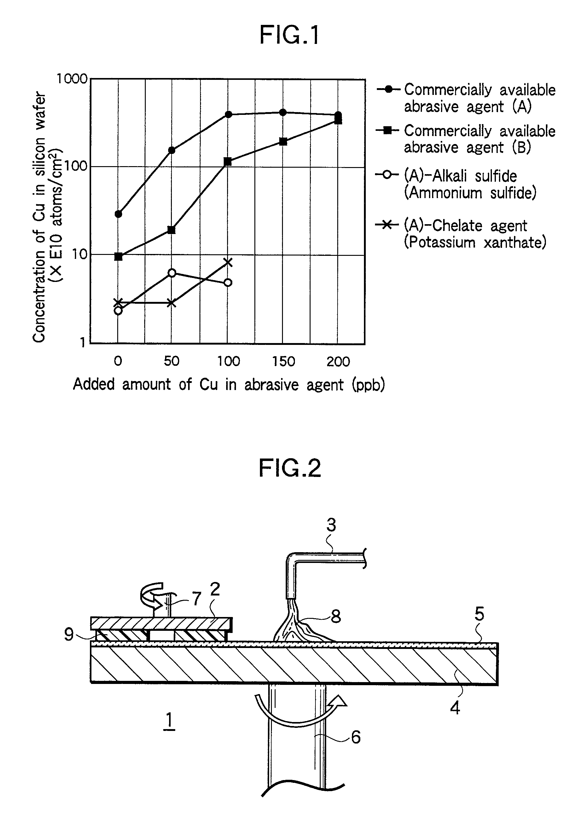
[0050] First, an abrasive agent employed in a method according to a second embodiment will be described. Hereinafter, the abrasive agent employed in the method according to the second embodiment will be referred to as "abrasive agent of the second embodiment".

[0051] An abrasive agent of the second embodiment contains silica, which is a principal ingredient, and potassium xanthate serving as a chelate agent. Thus, the difference of the second embodiment from the first embodiment in constituent element is that ammonium sulfide is replaced by potassium xanthate.

[0052] Other than the constituent element of abrasive agent, the second embodiment is the same as the first embodiment. Specifically, the abrasive agent of the second embodiment is prepared by adding potassium xanthate to a commercially available abrasive agent (A). The added amount of potassium xanthate is 0.001% by weight...


PUM


Abstract

Mirror-polishing of a silicon wafer is conducted using an abrasive agent which contains silica as a principal ingredient, and either one of the ingredients set forth at (1) and (2): (1) an ingredient which is selected from alkali sulfide, alkali hydrogensulfide, and the mixture thereof; and (2) a chelate agent which contains at least alpha-benzoinoxime, diethyldithiocarbamic acid, cupferron, xanthogenic acid, neocupferron, beryllon II, beta-quinolinol, 1,1,1-trifluoro-3(2-thenoyl)acetone, dimethylglyoxime, and 1-(2-pyridylazo)-2-naphthol.

Description

[0001] 1. Field of the Invention[0002] The present invention relates generally to a method of polishing silicon wafer. More specifically, it relates to a method of polishing a silicon wafer, by which contamination by a metal, such as copper, nickel, or the like, is prevented while the silicon wafer is being subjected to a mirror-polishing process.[0003] 2. Description of Related Art[0004] Usually, a silicon wafer is manufactured by slicing a single-crystal ingot into a wafer, and thereafter applying to the wafer the predetermined steps of chamfering, lapping, etching, mirror-polishing, and cleaning.[0005] At the mirror-polishing step (hereinafter, the mirror-polishing step is occasionally referred to simply as "polishing step"), in general, a silica-containing abrasive agent, which is alkaline aqueous solution containing fine (i.e., very small) silica (i.e., SiO.sub.2) abrasive grains dispersed therein, (referred to as "alkaline silica-containing abrasive agent") is used. In case of...

Claims


Application Information

Patent Timeline
IPC IPC(8): B24B57/02B24B37/00C09G1/02H01L21/304H01L21/306
CPCB24B37/044C09G1/02H01L21/02024
Inventor KAWASAKI, NOBUYUKIMORI, MASANORI
Owner SUMITOMO MITSUBISHI SILICON CORP
Why Eureka
Try Eureka