
Method and system for modifying and densifying a porous film

a technology of porous film and densification method, which is applied in the field of methods and systems for altering the porosity of thin films, can solve the problems of large time-consuming and laborious preparation of xerogels, small circuit layouts stacked in a multi-layer structure are susceptible to parasitic effects, and air does not lend itself to multi-layer design

Inactive Publication Date: 2001-11-08
ADVANCED MICRO DEVICES INC
View PDF0 Cites 14 Cited by
  • Summary
  • Abstract
  • Description
  • Claims
  • Application Information

AI Technical Summary

Benefits of technology

[0029] The process and material induced deleterious effects on the dielectric constant of a dielectric film formed with a xerogel can be reduced by the process and system of the present invention. By controllably reducing the porosity of the dielectric film, the present invention enables the formation of a densified dielectric film that resists the inter-diffusion of fabrication materials and process chemicals, and increases the hardness of the film, such that an improved planarization process can be carried out.

Problems solved by technology

With growing circuit speeds and miniaturization, smaller circuit layouts stacked in a multilayer structure are susceptible to the parasitic effect of capacitive coupling.
Unfortunately, air does not lend itself to multilayered design as it offers no underlying structure to support layered circuits.
Accordingly, the preparation of xerogels can require considerable time.

Method used


Image

  • Method and system for modifying and densifying a porous film
  • Method and system for modifying and densifying a porous film
  • Method and system for modifying and densifying a porous film

Examples


first embodiment

[0032] 1. First Embodiment

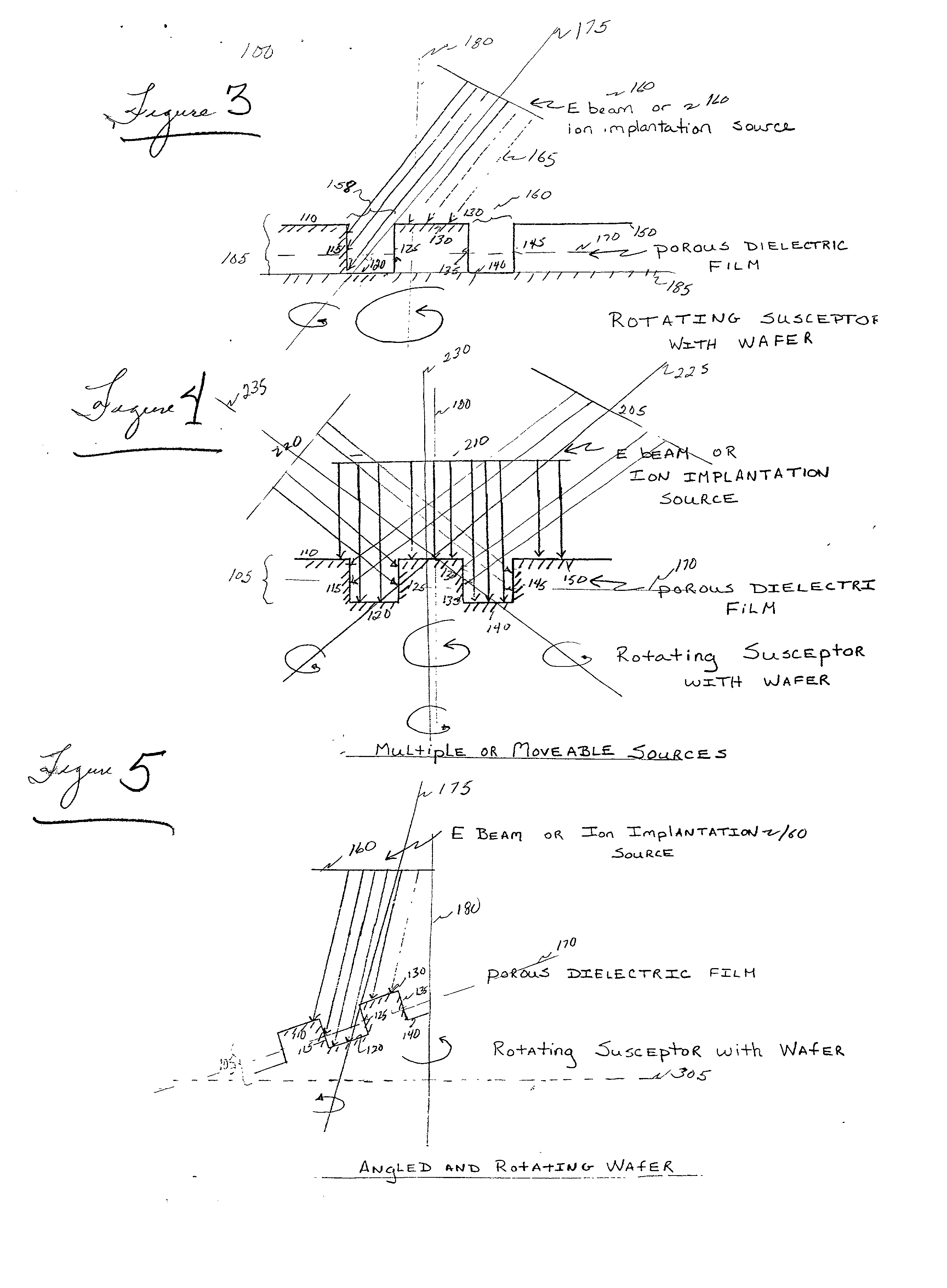
[0033] A tunable dielectric comprising the film 105 having a plurality of pores is shown in FIG. 3. Preferably, the film 105, which may be a thin film, is supported by an underlying structure 185, such as a semiconductor substrate with or without underlying process layers. Utilizing a radiation source 160 that can be rotated, inclined, and / or moved, one or more electron beams 165 are formed. In a first embodiment, an "Electron Cure 30" manufactured by Allied Signal Incorporated of San Diego, Calif. provides the radiation source 160. The electron beams 165 preferably radiate along one 175 or more beam axes. When the thin film 105 is placed at a processing position 100, the electron beams 165 irradiate one or more select areas of the thin film 105. In FIG. 3, the select areas comprise the second side wall 115 and the second substantially plane surface 130. In these areas 115 and 130, the electron beams 165 preferably form an acute radiating angle between the ...

second embodiment

[0036] 2. Second Embodiment

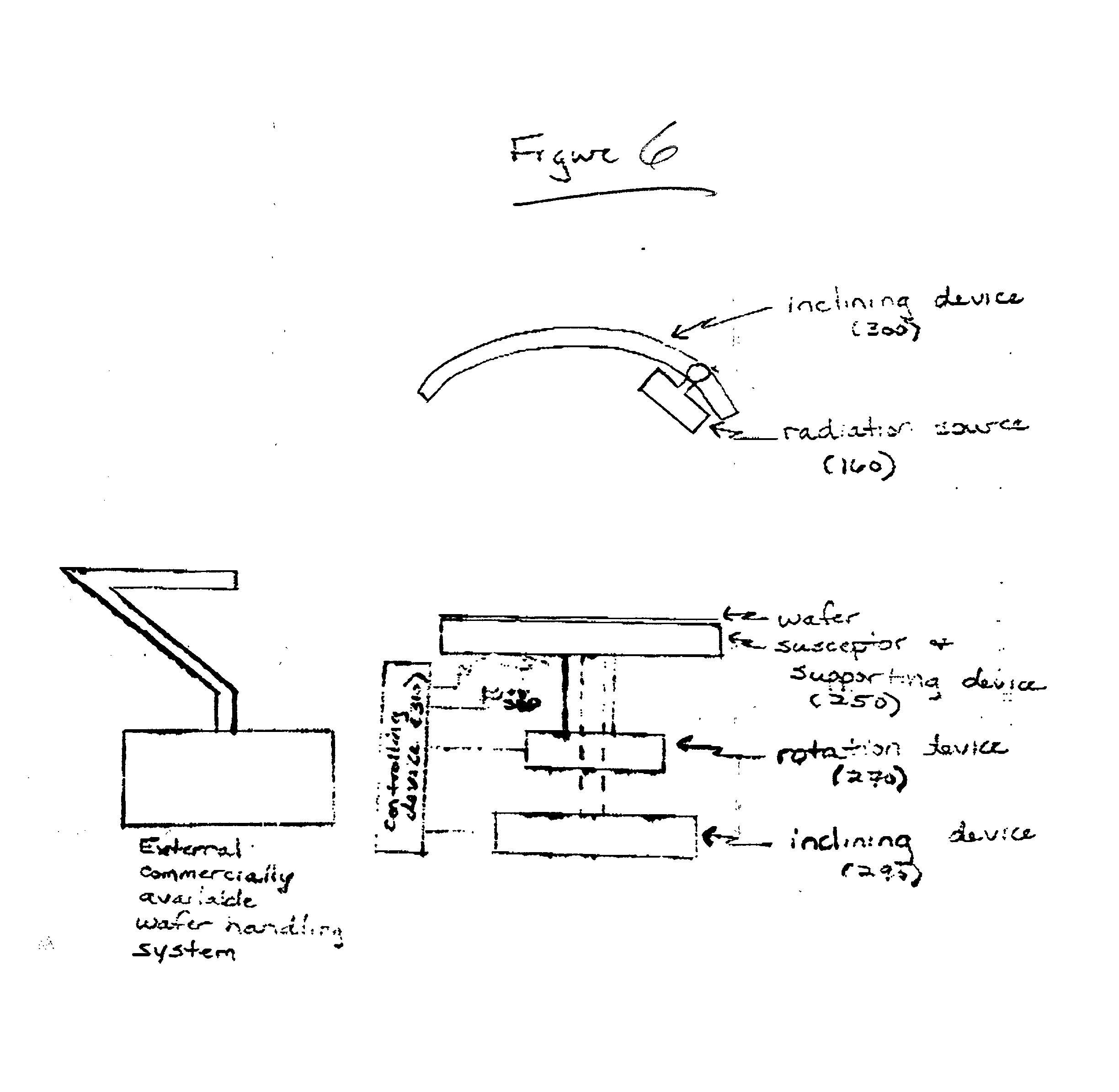
[0037] FIG. 4 shows a second embodiment that also reduces the porosity of thin film 105. Only those parts of the second embodiment that are different from the first embodiment will be described. As shown, the exposed surfaces of thin film 105 are irradiated from three distinct sources of radiation 205, 210, and 220. The three sources 205, 210, and 220 that are shown are focused at specific surfaces 110, 115, 120, 125, 130, 135, 140, 145, and 150 that collectively comprise the exposed surface. The second embodiment allows for the rotation of the radiation sources 205, 210, and 220 and the thin film 105 about a plurality of beam axes 225, 230, and 235 and a rotational axis 180, respectively. Moreover, the second embodiment allows the radiation sources 205, 210, and 220 and the thin film 105 to be inclined through a plurality of angles measured between the level horizontal surface 305 (shown in FIG. 5) and the beam axes 225, 230, and 235 and the level horizon...

third embodiment

[0038] 3. Third Embodiment

[0039] FIG. 5 depicts a modification of the first embodiment as it shows both a single movable radiation source 160 and illustrates the thin film 105 in an inclined and rotating state. As explained above, as the select areas of the thin film 105 are irradiated, the radiation source 160 and the thin film 105 are rotated to ensure even coverage of select areas 110, 115, 120, and 130. Likewise, the radiation source 160 and the thin film 105 may be inclined. Moreover, the rotation and the inclination of the radiation source 160 and the thin film 105 may continuously change, as the exposed surface is irradiated to ensure that the select areas 110, 115, 120, and 130 attain a predetermined dielectric constant.

[0040] Porous silica xerogels and aerogels were used as representative dielectric films in the above-described embodiments. However, those skilled in the art will appreciate that the invention envisions the use of other porous materials, such as, for example,...


PUM

PropertyMeasurementUnit
Pore sizeaaaaaaaaaa
Dielectric polarization enthalpyaaaaaaaaaa
Angleaaaaaaaaaa

Abstract

The invention provides a system and a method for densifying a surface of a porous film. By reducing the porosity of a film, the method yields a densified film that is more impenetrable to subsequent liquid processes. The method comprises the steps of providing a film having an exposed surface. The film can be supported by a semiconductor substrate. When the film is moved to a processing position, a focused source of radiation is created by a beam source. The exposed surface of the film is then irradiated by the beam source at the processing position until a predetermined dielectric constant is achieved. The film or beam source may be rotated, inclined, and / or moved between a variety of positions to ensure that the exposed surface of the film is irradiated evenly.

Description

[0001] 1. Technical Field of the Invention[0002] The invention relates to a method and a system for altering the porosity of thin films, and more particularly, to a method and a system for creating a dielectric film having a low dielectric constant.[0003] 2. Description of Related Art[0004] Microelectronic circuits perform a variety of functions in small designs. With growing circuit speeds and miniaturization, smaller circuit layouts stacked in a multilayer structure are susceptible to the parasitic effect of capacitive coupling.[0005] One solution that controls the effect of capacitive coupling employs an interlayer dielectric having a low dielectric constant. The integration of low dielectric constant materials between integrated circuits isolate conductors, reduces power consumption, and lowers the parasitic effect of capacitive coupling.[0006] Several materials can be used as dielectrics. One insulator used in microelectronic circuits is silicon dioxide (SiO.sub.2). Silicon dio...

Claims


Application Information

Patent Timeline
IPC IPC(8): H01L21/3105H01L21/314H01L21/316
CPCH01L21/02126H01L21/02203H01L21/02351H01L21/3105H01L21/31695
Inventor PANGRLE, SUZETTE K.HUANG, RICHARDPRAMANICK, SHEKHAR
Owner ADVANCED MICRO DEVICES INC
Learn More