Resonator, filter, duplexer, and communication device

a communication device and filter technology, applied in the direction of resonators, superconductors/hyperconductors, electrical devices, etc., can solve the problems of power loss due to edge effects inescapable, and the character of resonators is inevitably subject to deterioration

Inactive Publication Date: 2002-01-03
MURATA MFG CO LTD
View PDF0 Cites 67 Cited by
  • Summary
  • Abstract
  • Description
  • Claims
  • Application Information

AI Technical Summary

Problems solved by technology

Such a resonator constituted of one microstrip line has a drawback, in that characteristics thereof are inevitably subjected to deterioration caused by the edge effect which the microstrip line intrinsically possesses.
Even if the film-t

Method used


Image

  • Resonator, filter, duplexer, and communication device
  • Resonator, filter, duplexer, and communication device
  • Resonator, filter, duplexer, and communication device

Examples


first embodiment

[0046] Next, the configuration of the resonator in accordance with the present invention will be described with reference to FIGS. 5A-6A.

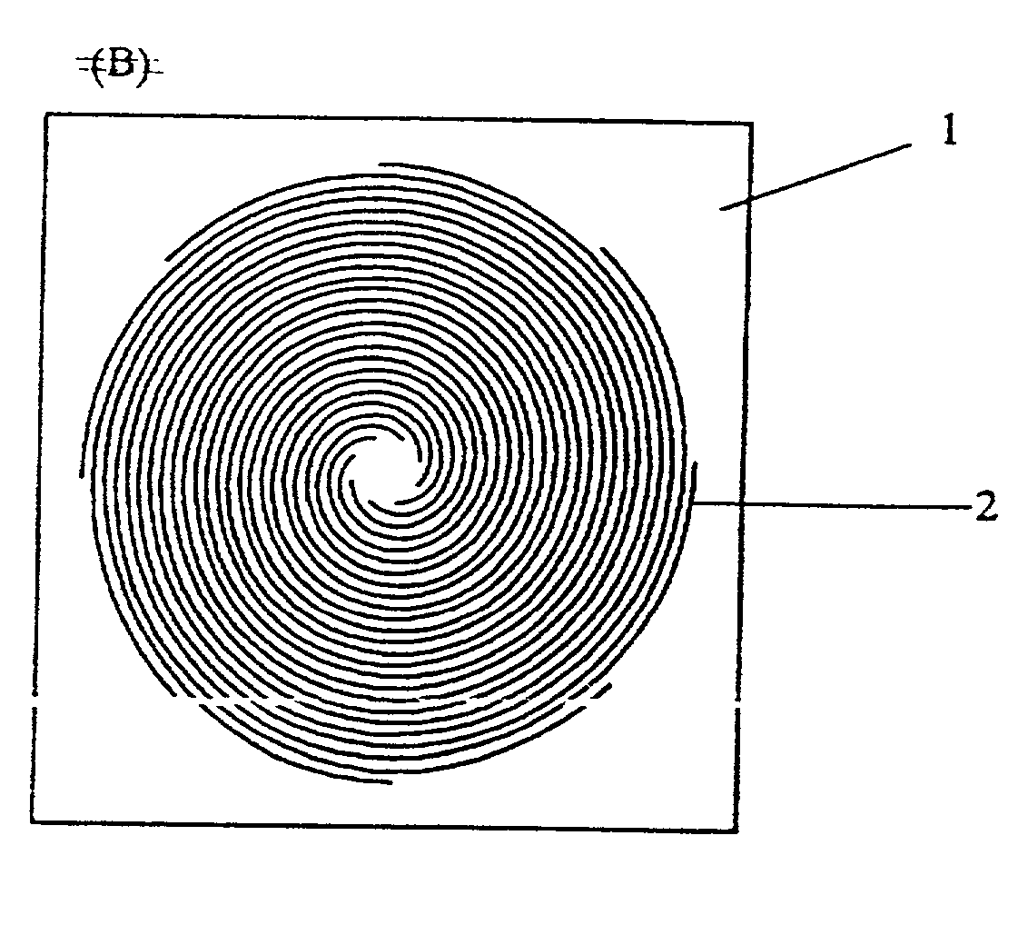
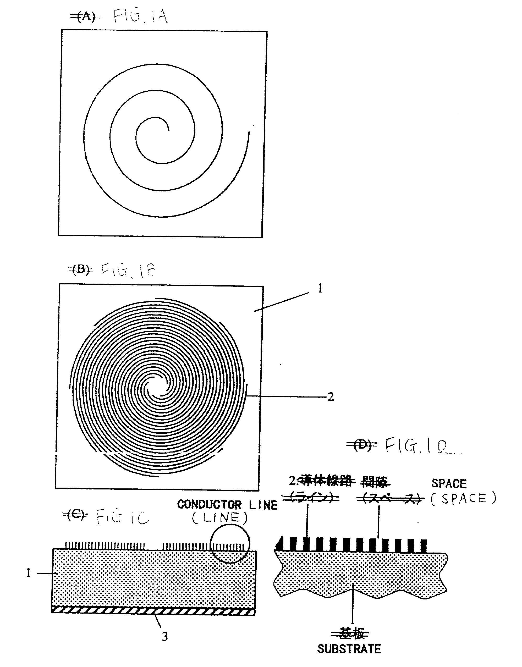
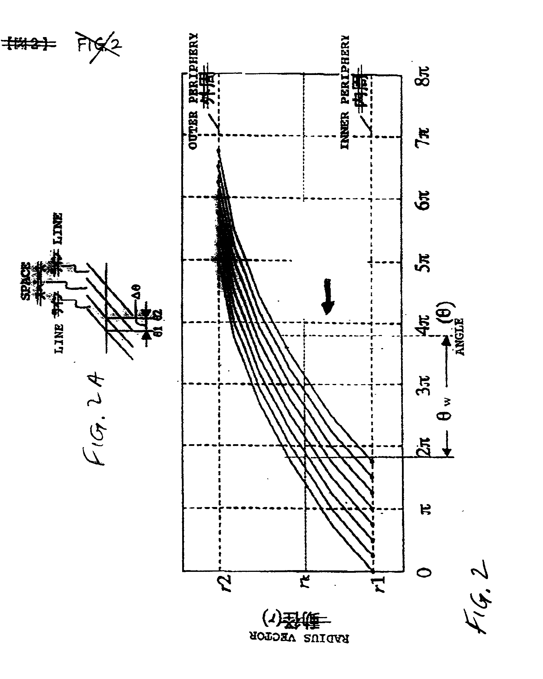
[0047] FIG. 5A is a top view of the resonator, FIG. 5B is a central vertical section, and FIGS. 5C and 5D are plan views of two line patterns. A ground electrode 3 is formed over the entire bottom surface of a dielectric substrate 1, and a plurality of spiral line patterns 21 are formed on the top surface. FIG. 5C is an example of the spiral line patterns, and a plurality of mutually congruent spiral lines 2 each of which has open ends at both ends, are arranged on the top surface of the dielectric substrate so as not to intersect one another in a manner such that first and second ends of each of the lines are rotation-symmetrically positioned around a predetermined point (the center point) on the substrate.

[0048] In FIG. 5B, reference numeral 5 denotes an insulating layer, and on the top surface thereof, a line pattern 22 different from the above-...

second embodiment

[0060] Next, the configuration of the resonator in accordance with the present invention will be described with reference to FIGS. 7A to 7D. FIG. 7A is a top view of the resonator, FIG. 7B is a central vertical section, and FIGS. 7C and 7D are plan views of two line patterns. A ground electrode 3 is formed over the entire bottom surface of a dielectric substrate 1, and on the top surface thereof, a multiple spiral line is formed of a line pattern 21 constituted of a plurality of spiral lines, as shown in FIG. 7C. This line pattern 21 is similar to the one shown in FIGS. 5A to 5D. In FIG. 7B, reference numeral 5 denotes an insulating layer, and a line pattern 23 is formed on the top surface of this insulating layer. FIG. 7D shows an example of this line pattern 23. Herein, first ends and second ends of a plurality of lines are each arranged substantially at inner and outer periphery portions around the same center point as the multiple spiral line formed of line pattern 21, and each ...

fourth embodiment

[0069] FIGS. 10A to 10D are views illustrating the configuration of a resonator in accordance with the present invention. FIG. 10A is a top view of this resonator, FIG. 10B is a central vertical section thereof. In this example, multiple spiral patterns 21a, 23a, 21b, and 23b are successively laminated on the top surface of the dielectric substrate 1 with an insulating layer interposed therebetween. Of these four line patterns, 21a and 21b are left-handed spiral lines, as shown in FIG. 10C. On the other hand, 23a and 23b are right-handed spiral lines, as shown in FIG. 10C. If we consider the two layered multiple spiral lines shown in FIGS. 7A to 7D as one set, the above-described structure will equal two sets of these two layered multiple spiral lines. Such a multilayer lamination allows the storage amount of electric field energy to further enhanced, and enables magnetic field energy to be kept at a low loss. This results in a more increased Q value.


PUM


Abstract

A resonator, a filter, and a duplexer are provided which are capable of very effectively suppressing the power loss caused by the edge effect, and which allow a great reduction in the overall size to be achieved. Also, a communication device including the above-mentioned filter or duplexer is provided. A ground electrode is formed over the bottom surface of a dielectric substrate, and a multiple spiral line pattern is formed on the top surface thereof. A radial line pattern is further formed on this surface with an insulation layer interposed therebetween. By thus disposing the radial pattern adjacently to the multiple spiral resonator constituted of the above-mentioned multiple spiral line, an electrostatic capacitance is added to the multiple spiral resonator. This reduces the occupation area of the resonator on the substrate, and improves the loss reduction effect.

Description

[0001] 1. Field of the Invention[0002] The present invention relates to a filter, a duplexer, and a communication device for use in radio communication or the transmission / reception of electromagnetic waves, in e.g. a microwave band or a millimeter wave band.[0003] 2. Description of the Related Art[0004] An example of a miniaturizable resonator for use in a microwave band or millimeter wave band is a spiral resonator, disclosed in Japanese Unexamined Patent Application Publication No. 2-96402. This spiral resonator is able to fit a longer resonance line in a given occupation area by forming the resonance line into a spiral shape, thereby achieving its overall size-reduction.[0005] In such a conventional resonator, one half-wavelength line constitutes one resonator. Therefore, in a conventional resonator, the region where electrical energy is concentrated and stored, and the region where magnetic energy is concentrated and stored are separated from each other, and they are unevenly d...

Claims


Application Information

Patent Timeline
IPC IPC(8): H01P1/203H01P1/213H01P7/08
CPCH01P1/20381H01P1/2135H01P7/082H01P7/08
Inventor HIDAKA, SEIJIOTA, MICHIAKIFUJII, YASUOABE, SHIN
Owner MURATA MFG CO LTD
Why Eureka
Try Eureka