Chemical vapor deposition using organometallic precursors

a technology of organometallic precursors and chemical vapor deposition, which is applied in chemical vapor deposition coating, solid-state devices, coatings, etc., can solve the problems of high dielectric constant, low dielectric constant, and insufficient dielectric constant of materials,

Inactive Publication Date: 2002-01-24
MICRON TECH INC
View PDF0 Cites 105 Cited by
  • Summary
  • Abstract
  • Description
  • Claims
  • Application Information

AI Technical Summary

Problems solved by technology

However, these materials may not possess dielectric constants that are sufficiently high to meet the design requirements for more advanced semiconductor devices.
However, these alternatives have not proved satisfactory due to shortcomings of one kind or another.
For example, titanium dioxide (TiO.sub.2) has a high dielectric constant but also has a relatively high current leakage compared to SiO.sub.2 and Si.sub.3N.sub.4.
Consequently, TiO.sub.2 is typically unsuitable for use in high density semiconductor devices due to the adverse effects of current leakage.
However, this method has several drawbacks and fails to provide a satisfactory dielectric insulating layer for high density semiconductor devices.
The use of TiCl.sub.4 as a titanium source results in the formation of chlorine related impurities in the dielectric film.
These impurities are undesirable because chlorine has many adverse qualities, including being an etchant to SiO.sub.2, as well as being corrosive.
In addition, the use of plasma CVD limits the range of applications for which this dielectric material may be used.
Although plasma CVD methods may be employed at lower temperatures than traditional non-plasma methods, they typically produce poor step coverage when used to coat high aspect ratio devices.
Therefore, this method does not reliably produce conformal films and thus, is not typically suitable for use in manufacturing modem high aspect ratio devices, such as DRAMs.
The use of plasma deposition techniques is also known to create damage centers which induce high leakage in deposited dielectric films.
Plasma processes also tend to incorporate hydrogen and other contaminants into the film, thereby further degrading quality and performance of semiconductor devices.
However, MOCVD processes have not been used for depositing multi-component oxide materials such as mixed phase titanium silicon oxide dielectrics.

Method used


Image

  • Chemical vapor deposition using organometallic precursors
  • Chemical vapor deposition using organometallic precursors
  • Chemical vapor deposition using organometallic precursors

Examples


Embodiment Construction

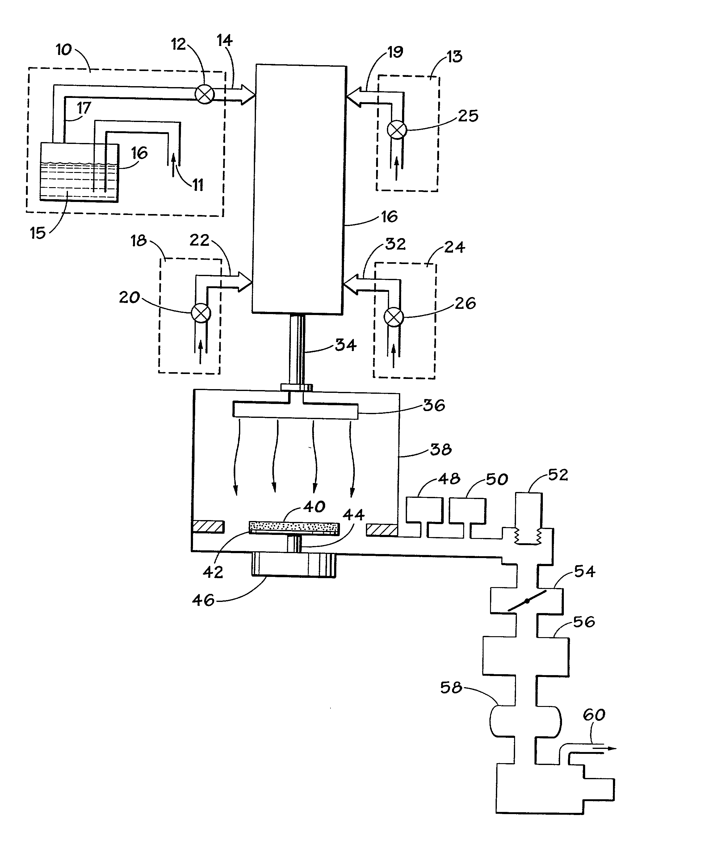
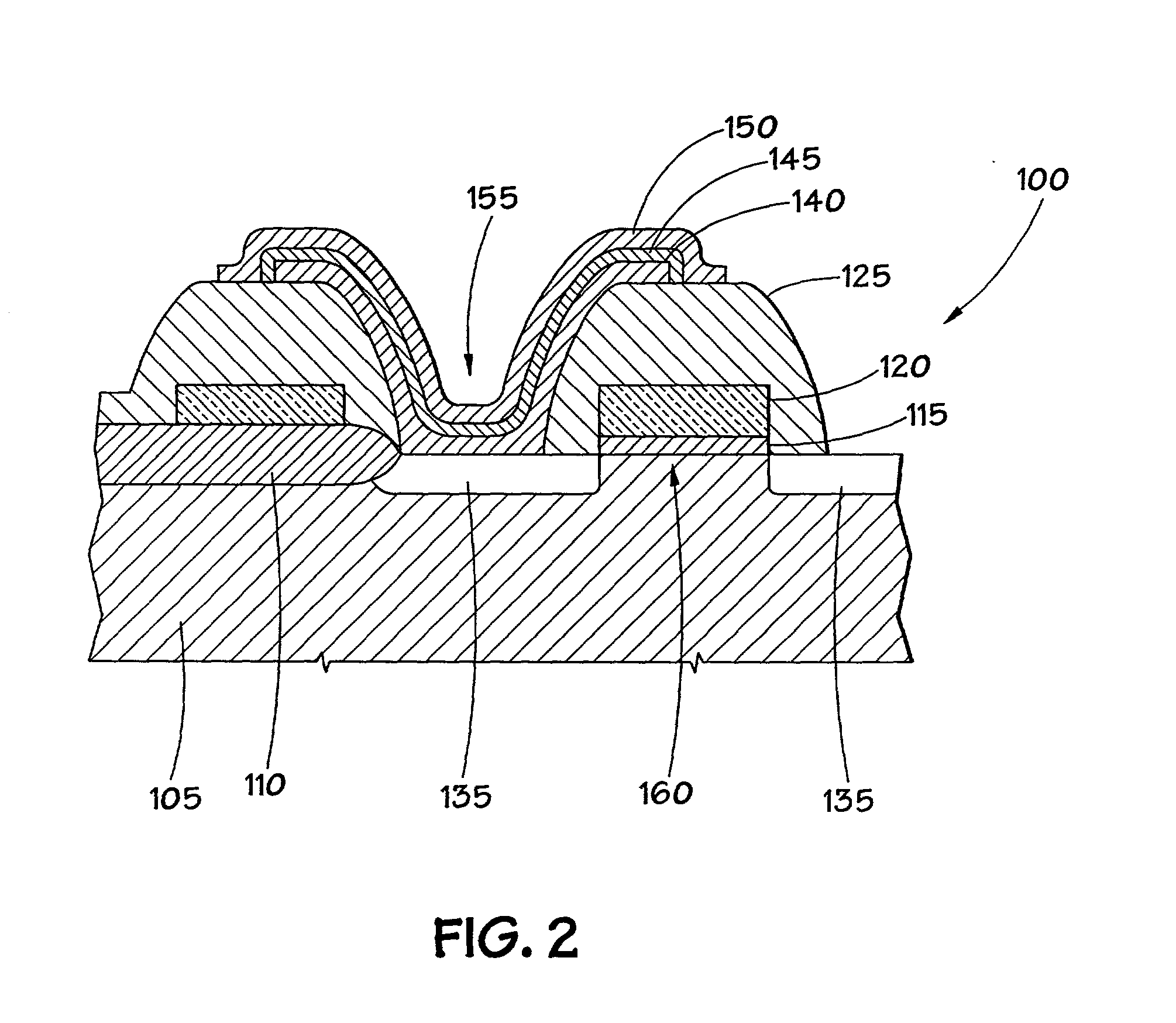
[0016] As used herein, the term "substrate" refers to any semiconductor substrate, such as, for example, a semiconductor wafer substrate of silicon or GaAs. It will be understood by those skilled in the art that the term "substrate" may include either a semiconductor wafer or the wafer along with various process layers formed on the wafer. The term "metals" is defined to include metals, refractory metals, intermetallics or combinations thereof. The term "film" may be used interchangeably with the term "layer".

[0017] In embodiments of the disclosed method, highly reactive organic sources of metal may be used to deposit conformal multi-component films, including multi-component oxide films and multi-component nitride films, on semiconductor surfaces. Deposited films may include mixed phase dielectric and conductive films. By "multi-component film" it is mean that a film is comprised of at least one dielectric and / or conductive compound in combination with another material. Examples of...


PUM

PropertyMeasurementUnit
pressureaaaaaaaaaa
temperatureaaaaaaaaaa
pressureaaaaaaaaaa

Abstract

A multi-component layer is deposited on a semiconductor substrate in a semiconductor process. The multi-component layer may be a dielectric layer formed from a gaseous titanium organometallic precursor, reactive silane-based gas and a gaseous oxidant. The multi-component layer may be deposited in a cold wall or hot wall chemical vapor deposition (CVD) reactor, and in the presence or absence of plasma. The multi-component layer may also be deposited using other processes, such as radiant energy or rapid thermal CVD.

Description

[0001] 1. Field of the Invention[0002] This invention relates generally to semiconductor processing and, more specifically, to chemical vapor deposition processes for semiconductors. In particular, this invention relates to chemical vapor deposition of dielectric and other materials using organometallic precursors.[0003] 2. Description of the Related Art[0004] With reduction in semiconductor device sizes and a corresponding increase in circuit complexity, the need has grown for reliable dielectric materials having high dielectric constants. Traditionally, silicon-based dielectrics, such as silicon dioxide (SiO.sub.2) and silicon nitride (Si.sub.3N.sub.4), have been used to form insulating layers in semiconductor devices, including dynamic random access memory chips (DRAMs). These silicon-based materials have been popular because they exhibit low current leakage and a high resistance to breakdown. However, these materials may not possess dielectric constants that are sufficiently hig...

Claims


Application Information

Patent Timeline
Patent Type & Authority Applications(United States)
IPC IPC(8): C23C16/40H01L21/316H01L21/8242
CPCC23C16/40H01L21/31604H01L27/10852H01L21/02164H01L21/02183H01L21/02178H01L21/02205H01L21/022H01L21/02271H01L21/02211H01L21/02186H01L21/0217H10B12/033
Inventor SANDHU, GURTEJ S.FAZAN, PIERRE
Owner MICRON TECH INC
Why Eureka
Try Eureka