
Device for opto-electrical acquisition of shapes by axial illumination

a technology of axial illumination and optical acquisition, applied in the field of transceivers, can solve the problems of inaccessibility and untestability of parameters, difficulty in applying digital signal processing (dsp) technology to ir communication in this conventional ir transceiver receiving chain, transceiver is incapable of providing an analog signal without risking the disruption of the operation of the receiver chain,

Inactive Publication Date: 2002-01-31
IBM CORP
View PDF0 Cites 2 Cited by
  • Summary
  • Abstract
  • Description
  • Claims
  • Application Information

AI Technical Summary

Benefits of technology

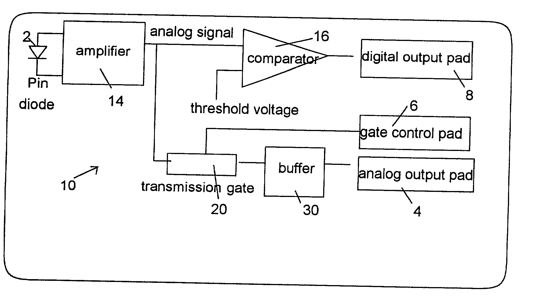
[0011] According to the invention, a transmission gate and unity gain buffer are interposed between the amplifier output and an analog output pad. The transmission gate behaves as a switch, passing the analog output signal to the analog output pad only when an analog output is required. For example, to use the analog output signal for digital signal processing, for a relatively strong signal, it is unnecessary to use digital signal processing and the transmission gate remains off. For a relatively weak signal, the transmission gate is turned on, thereby passing the analog signal to the unity gain buffer which provides an analog signal output to the DSP device. Thus, the transmission gate minimizes the effect of the isolated analog output, and further serves as a switch and multiplexer which allows a single isolated analog output to be connected to different test points through the use of multiple transmission gates.
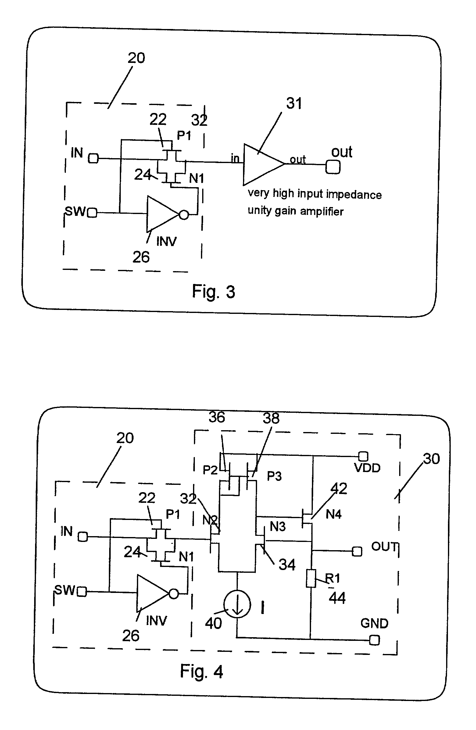
[0018] In a further aspect of the invention, a transmission gate for selectively blocking or passing the analog input signal to the buffer is provided. The transmission gate includes at least one transistor which selectively blocks or passes the analog input signal responsive to a level of a gate voltage. In a preferred embodiment, the transmission gate includes a P-type FET and an N-type FET with sources (or drains) of the P-type FET and the N-type FET connected to the circuit input and drains (or sources) of the P-type FET and the N-type FET connected to an input of the buffer, a gate of one of the P-type FET and N-type FET being connected to a switching signal through an inverter. Since the source and drain of a P-type FET and an N-type FET are symmetrical and exchangeable, the connections of the sources and drains can be reversed without affecting the operation of the transmission gate.

Problems solved by technology

Thus, these parameters are inaccessible and untestable.
Hence, it is very difficult to apply digital signal processing (DSP) technology to IR communication in this conventional IR transceiver receiving chain.
However, DSP usually requires an analog signal in order to effect the analog-to-digital conversion, and a conventional IR transceiver is incapable of providing an analog signal without risking disruption of the operation of the receiver chain.
Furthermore, the conventional IR transceiver is difficult to test and debug.
However, because the analog signal is not accessible, when the device malfunctions or experiences product quality problems common diagnostic procedures are largely unavailable because the analog signal output of the amplifier is untestable.
However, since in an integrated circuit design the load capability of an amplifier is limited due to restrictions in the chip die size, this is significantly more complex than merely adding a connection from an analog output pad to the amplifier output.
A direct connection from the amplifier output to an analog output pad would add an additional load on the amplifier output which would affect the receiver chain performance.
The extra load results not only from the parasitic capacitance of the connection trace and the pad, but also from the input impedance of external components such as a DSP device or measurement instrument.
If the additional load is too heavy, the IR transceiver performance will be degraded.
In extreme cases (e.g., where a large capacitance is added to the amplifier output), a conventional IR transceiver will oscillate and system failure will result.

Method used


Image

  • Device for opto-electrical acquisition of shapes by axial illumination
  • Device for opto-electrical acquisition of shapes by axial illumination
  • Device for opto-electrical acquisition of shapes by axial illumination

Examples


Embodiment Construction

[0026] Turning now to the drawings and more specifically to FIGS. 2-4, a preferred embodiment of the present invention will be described.

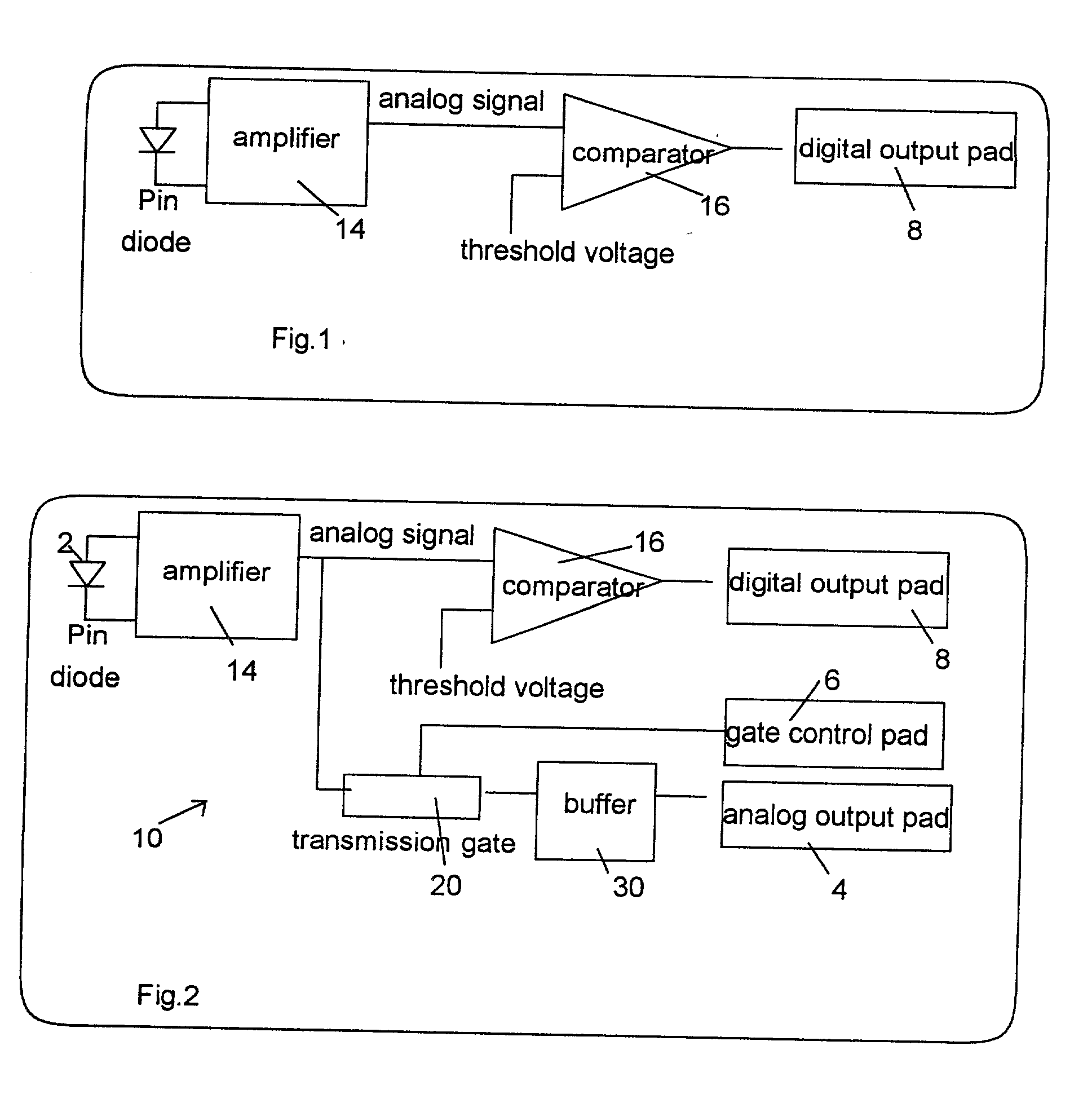
[0027] FIG. 2 illustrates a receiver chain 10 in a photoelectric transceiver according to the invention. A photodiode such as a PIN diode 2 generates an electrical current proportional to the optical energy of an infrared optical signal received by the PIN diode 2. A conventional amplifier 14 converts the electric current to voltage and magnifies the voltage, which is output to comparator 16. A reference voltage at a selected threshold level is applied to the reference input of the comparator 16. When the analog output signal of the amplifier 14 exceeds the reference voltage, the comparator 16 emits a digital pulse for the duration of the interval during which the analog output signal of the amplifier 14 exceeds the reference voltage, which is transmitted to a digital device (not shown) through digital output pad 8. At all other times, the comparat...


PUM


Abstract

An infrared (IR) transceiver having a receiver chain with an isolated analog output, includes a transmission gate and a unity gain buffer interposed between the amplifier output and an analog output pad. The transmission gate behaves as a switch, passing the analog output signal to the analog output pad only when an analog output is required. The unity gain buffer has a high input resistance, a low input capacitance, a unity gain and a low output impedance, so that the load of a digital signal processing (DSP) device or measuring instrument on the analog output pad is isolated and does not affect the performance of the receiver chain. Since the transfer rates of the transmission gate and the buffer are each unity, the analog output pad provides a high fidelity analog output signal to the output buffer.

Description

[0001] 1. Field of the Invention[0002] The present invention relates to transceivers, and more particularly to an infrared digital transceiver having an isolated analog output.[0003] 2. Description of the Related Art[0004] Conventional digital infrared (IR) transceivers provide only a digital output. The receiver component of the transceiver converts infrared optical pulses into discrete electrical pulses for downstream processing.[0005] FIG. 1 illustrates a conventional IR transceiver receiving chain. A photodiode (unreferenced) such as a PIN diode converts the optical energy from an infrared optical signal to an electric current. An amplifier 14 converts the electric current to voltage and magnifies the voltage. The output (analog signal) of the amplifier 14 is fed to a comparator input and a threshold voltage is applied to the other input of the comparator 16.[0006] When the analog output signal of the amplifier 14 is greater than the threshold voltage, the comparator 16 emits a ...

Claims


Application Information

Patent Timeline
IPC IPC(8): H04B10/40
CPCH04B10/697
Inventor FENG, KAI D.
Owner IBM CORP
Learn More