

Process for producing a chip
a technology of a chip and a process, which is applied in the direction of chemistry apparatus and processes, transportation and packaging, and other domestic objects, can solve the problems of unsatisfactory torque of the apparatus, difficult adjustment dependent, and torn pressure sensitive adhesive sheets, and achieve uniform chip spacing and productivity enhancement. , the effect of satisfying the requiremen
- Summary
- Abstract
- Description
- Claims
- Application Information
AI Technical Summary
Benefits of technology
Problems solved by technology
Method used
Image

Examples
example 1
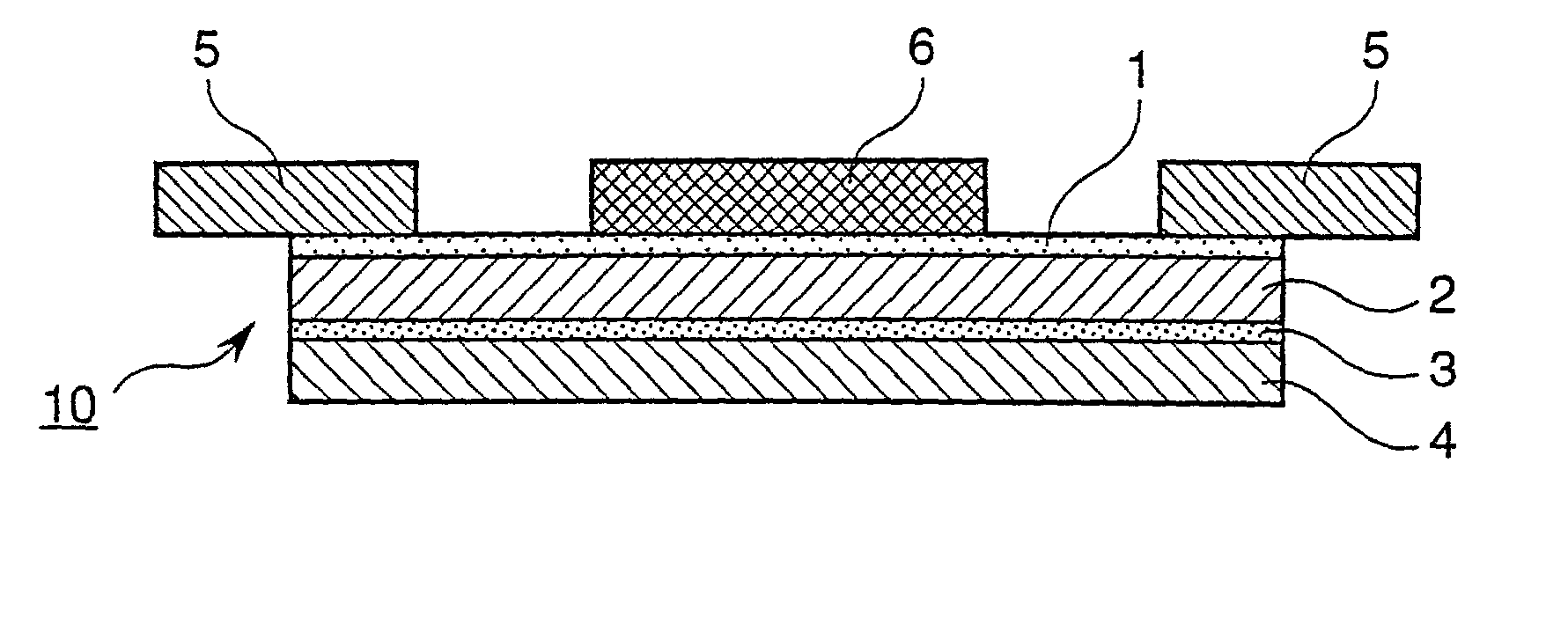
[0078] 1(1) Production of pressure sensitive adhesive 1 for setting the object:
[0079] 100 parts by weight of an acrylic pressure sensitive adhesive (copolymer of n-butyl acrylate and acrylic acid), 200 parts by weight of a urethane acrylate oligomer having a molecular weight of 7000, 10 parts by weight of a crosslinking agent (isocyanate type) and 10 parts by weight of an ultraviolet curable reaction initiator (benzophenone type) were mixed together, thereby obtaining an ultraviolet curable pressure sensitive adhesive composition for setting the object.
[0080] 1(2) Adhesive 3 for films bonding:
[0081] A polyurethane type adhesive (elastic modulus of 3.0.times.10.sup.8 N / m.sup.2) was used as the adhesive for films bonding.
[0082] 1(3) Lamination of shrinkable film and expansible film:
[0083] An expansible ethylene / methacrylic acid copolymer film (having a thickness of 100 .mu.m and an elastic modulus of 2.15.times.10.sup.8 N / m.sup.2) was coated with the adhesive of step 1(2) above so tha...
example 2
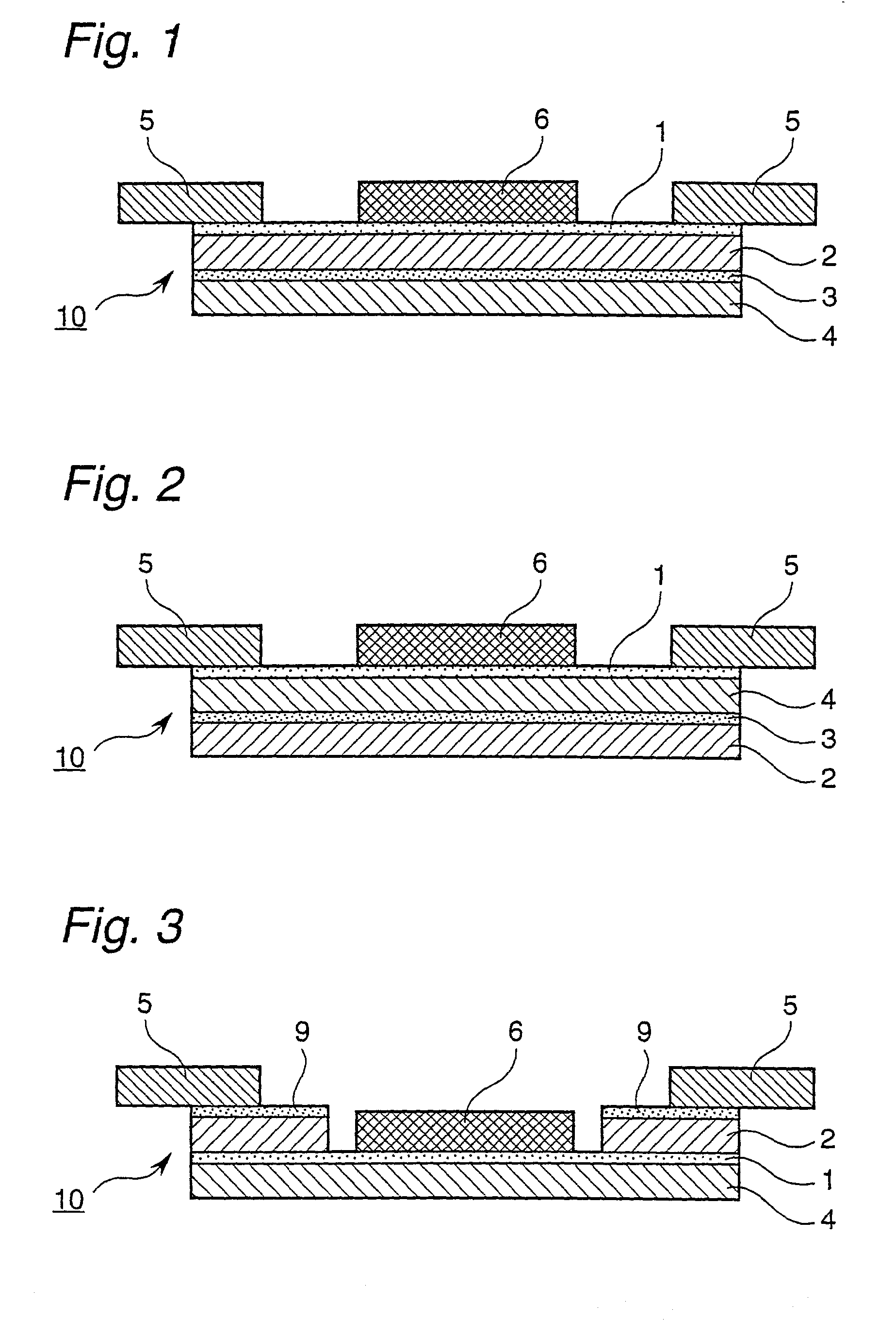
[0087] 2(1) Production of pressure sensitive adhesive 1 for setting the object:
[0088] An ultraviolet curable pressure sensitive adhesive composition was produced in the same manner as in step 1(1) of Example 1.
[0089] 2(2) Lamination of shrinkable film to pressure sensitive adhesive layer:
[0090] A 25 .mu.m thick polyethylene terephthalate film having undergone release treatment was coated with the pressure sensitive adhesive composition obtained in step 2(1) above so that the thickness of the coating was 10 .mu.m and heated at 100.degree. C. for 1 min. Thereafter, a thermally shrinkable polyethylene terephthalate film (having a thickness of 30 .mu.m and a shrinkage ratio of 50% at 120.degree. C.) was bonded to the pressure sensitive adhesive side of the coated polyethylene terephthalate film, thereby obtaining a shrinkable film having a pressure sensitive adhesive layer.
[0091] 2(3) Production of adhesive for films bonding:
[0092] 100 parts by weight of an acrylic pressure sensitive ad...
example 3
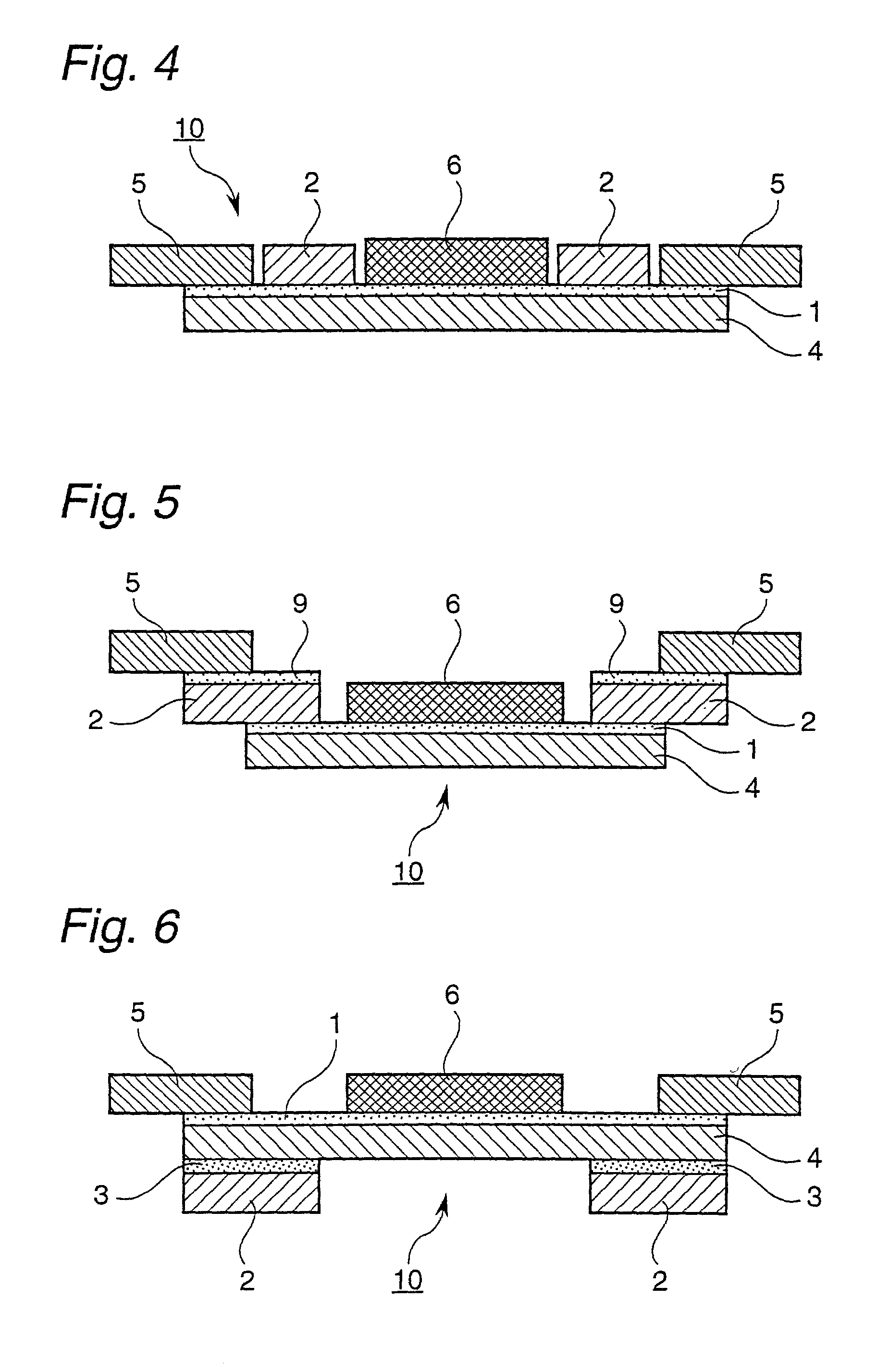
[0098] A peelable type pressure sensitive adhesive sheet for producing chip was produced in the same manner as in Example 2, except that a peelable type pressure sensitive adhesive composition comprising 100 parts by weight of an acrylic pressure sensitive adhesive (copolymer of n-butyl acrylate and 2-hydroxyethyl acrylate) and 10 parts by weight of a crosslinking agent (isocyanate type) was used as the pressure sensitive adhesive composition for setting the object.
[0099] The results are given in Table 1.
PUM
| Property | Measurement | Unit |
|---|---|---|
| Pressure | aaaaa | aaaaa |
| Sensitivity | aaaaa | aaaaa |
| Elastic modulus | aaaaa | aaaaa |
Abstract
Description
Claims
Application Information