Pulse reverse electrodeposition for metallization and planarization of semiconductor substrates

Inactive Publication Date: 2002-03-21
INVENSAS CORP
View PDF6 Cites 26 Cited by
  • Summary
  • Abstract
  • Description
  • Claims
  • Application Information

AI Technical Summary

Benefits of technology

[0013] A further object is to provide a method for depositing metal from an electrolytic bath onto a substrate while preventing excessive deposition at corners and protuberances of the substrate.

Problems solved by technology

When VLSI devices are prepared by the damascene process, which requires that the conducting metal be deposited into trenches formed in a layer of insulating material, it has been found difficult to achieve void-free metal deposits in trenches having high aspect ratios by PVD or CVD.
However, it has proved difficult to prepare void-free, and inclusion-free deposits in trenches of high aspect ratio.
The excess copper must then be removed by chemical-mechanical polishing (CMP), which is a time-consuming process that also generates substantial amounts of waste slurries that require careful and expensive disposal procedures.
However, because of the tendency of electroplating procedures to deposit excess metal at the edges of the wafer, it has proved difficult to prepare perfectly uniform layers of copper.
However, such procedures require additional equipment and are evidently wasteful of copper metal.

Method used


Image

  • Pulse reverse electrodeposition for metallization and planarization of semiconductor substrates
  • Pulse reverse electrodeposition for metallization and planarization of semiconductor substrates
  • Pulse reverse electrodeposition for metallization and planarization of semiconductor substrates

Examples


Embodiment Construction

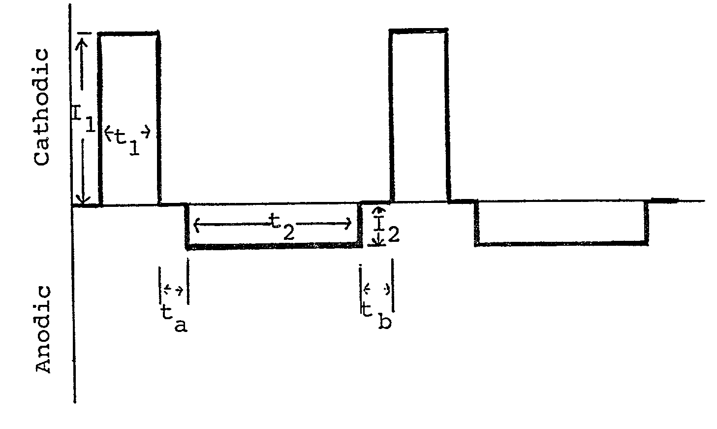
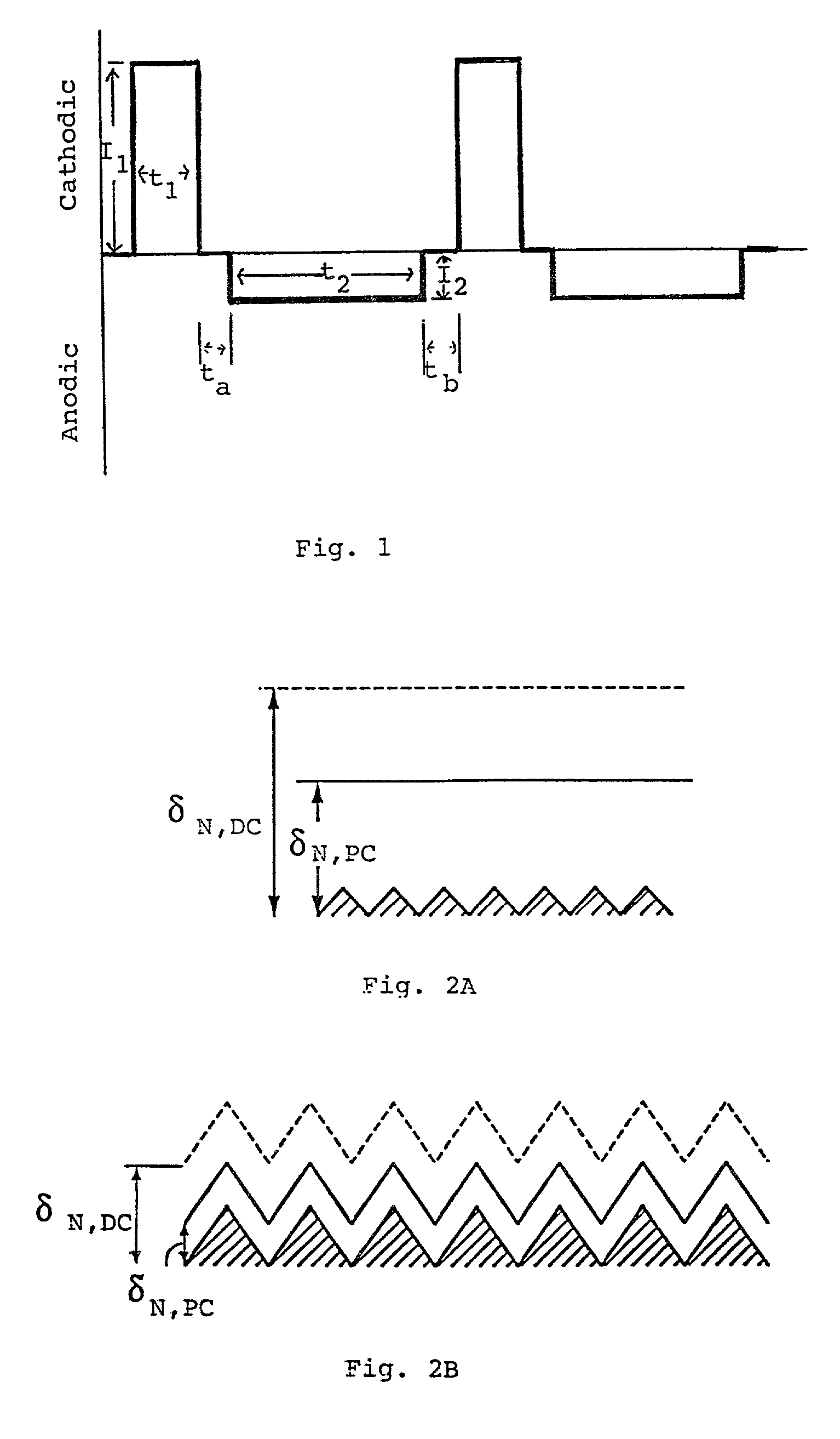
[0033] The distribution of metal electrodeposited on an electrically conductive substrate is determined by the local variations in the electrical current density. The primary current density in an electroplating cell is determined by the geometry of the electrodes. Typically, the primary current density is inversely proportional to the distance between the cathode and the anode along the path that the current follows between the electrodes.

[0034] When a voltage is first applied to the electroplating cell, the metal ions in solution in contact with the cathode are deposited on the cathode and the concentration of the ions in the adjacent solution decreases. Consequently, a concentration gradient is established near the cathode, and metal ions accordingly diffuse from the bulk solution region of relatively high concentration toward the depleted region adjacent to the cathode. This layer of depleted and variable metal ion concentration is the Nernst diffusion layer. In direct-current (...


PUM

PropertyMeasurementUnit
Fractionaaaaaaaaaa
Fractionaaaaaaaaaa
Fractionaaaaaaaaaa

Abstract

A smooth layer of a metal is electroplated onto a microrough electrically conducting substrate by immersing the substrate and a counterelectrode in an electroplating bath of the metal to be electroplated and passing a modulated reversing electric current between the electrodes. The current contains pulses that are cathodic with respect to said substrate and pulses that are anodic with respect to said substrate. The cathodic pulses have a duty cycle less than about 50% and said anodic pulses have a duty cycle greater than about 50%, the charge transfer ratio of the cathodic pulses to the anodic pulses is greater than one, and the frequency of said pulses ranges from about 10 Hertz to about 12000 Hertz. The plating bath is substantially devoid of levelers and may be devoid of brighteners.

Description

[0002] 1. Field of the Invention[0003] This invention relates to electrodeposition of metals and more particularly to electrodeposition of metals into microscopic recesses on the surface of a substrate and formation of uniform layers of electrodeposited metal on a substrate.[0004] 2. Brief Description of the Prior Art[0005] The manufacture of semiconductor devices, especially very large scale integrated (VLSI) chips is driven by technical and economic considerations toward the production of devices comprising greater numbers of transistors and associated circuits on a single semiconductor chip or wafer. The most complex chips manufactured today have a few million transistors on a semiconductor chip no larger than several millimeters on a side. The electrical interconnections between the transistors in such chips are provided by fine wires of a conductive metal extending in channels formed horizontally and vertically in the body of the chip. Conventionally, these electrical connectio...

Claims


Application Information

Patent Timeline
IPC IPC(8): C25D3/38C25D5/18H01L21/288H01L21/768H05K3/42
CPCB23H5/08B23H2300/12C25D3/38Y10T428/12396H01L21/2885H01L21/76877H05K3/423C25D5/18C25D5/611C25D5/617C25D5/627
Inventor TAYLOR, E. JENNINGSZHOU, CHENGDONGSUN, JENNY J.
Owner INVENSAS CORP
Why Eureka
Try Eureka