Method of manufacturing substrate having transparent conductive film, substrate having transparent conductive film manufactured using the method, and touch panel using the substrate

a technology of transparent conductive film and manufacturing method, which is applied in the direction of conductive layers on insulating supports, instruments, non-metal conductors, etc., can solve the problems of surface resistance of ito film, touch panel manufactured using such a substrate will not function properly, and the same kind of discrepancy is prone to occur again

Inactive Publication Date: 2002-03-21
NIPPON SHEET GLASS CO LTD
View PDF0 Cites 17 Cited by
  • Summary
  • Abstract
  • Description
  • Claims
  • Application Information

AI Technical Summary

Problems solved by technology

Of these steps, in a printing step such as silver ink printing or insulating ink printing and in the heat sealing step, heat treatment at a maximum temperature of 160.degree. C. is carried out, and during this heat treatment the surface resistance of the ITO film changes; as a result, in some cases a touch panel manufactured using such a substrate will not function properly.
Specifically, when the surface resistance of the ITO film has dropped due to heat treatment, the detected voltage drops and thus a discrepancy arises between the input position and the detected position; when the surface resistance has risen, the detected voltage rises and thus the same kind of discrepancy again becomes prone to occur.
Moreover, if the surface resistance distribution is not uniform, then the potential gradient loses its linearity as shown in FIG. 4B, that is, there is no longer a linear relationship between distance and potential, and hence it becomes impossible to detect the input position accurately.
With such an existing sputtering device, it is difficult to keep the above-mentioned percentage change in the surface resistance of the ITO film down to no more than .+-.10% under typical conditions used conventionally when manufacturing a transparent conductive film for an LCD (for example, substrate temperature: 200 to 400.degree. C.
60-minute heat resistance tests that the percentage change in the surface resistance was kept down to within -10% to +19%, but there is a problem that this is still insufficient.
Moreover, in the case of the latter of the above methods, there is a problem in that during the application of the coating solutions it is impossible to avoid foreign particles getting into the coating solutions and then during the baking there is a high probability of these foreign particles sticking, and a problem in that the percentage change in the surface resistance cannot be kept down to within .+-.20%, which is insufficient.
In FIG. 2A, when the oxygen proportion is below 0.016, the lower limit of the suitable range, there is a lack of oxygen resulting in an ITO film with many oxygen defects and poor crystallinity, and hence the mobility is extremely low.
Moreover, when there are oxygen defects in this way, electrons are not ejected and hence the carrier density is low.
Furthermore, when the tin (Sn) in the tin oxide added to the target is taken into the ITO film during the sputtering, if the ITO film has poor crystallinity in this way, then the amount of Sn taken into the ITO film is low, resulting in a low carrier density.
Oxidation and crystallization of the ITO film proceed during this heat treatment, with the number of oxygen defects falling and the amount of Sn taken into the ITO film increasing.
However, when most of the oxygen defects are filled in in this way, the effect of ejection of electrons is no longer obtained, and hence the carrier density decreases progressively with increasing oxygen proportion.
However, when the number of oxygen defects decreases in this way, the effect of ejection of electrons decreases and hence the carrier density drops.
As described above, when the proportion of oxygen in the mixed gas is increased during ITO film formation and when heat treatment is carried out while manufacturing an analog detection type touch panel, oxidation and crystallization of the ITO film proceed and the number of oxygen defects decreases.
However, the carrier density, which is also inversely proportional to the surface resistance, is small when the ITO film has a crystal structure containing many oxygen defects as shown in FIG. 2A due to ejection of electrons not occurring, but also becomes small when the ITO film has a crystal structure in which most of the oxygen defects are filled in as shown in FIG. 2C due to the effect of the ejection of electrons no longer being obtained.
An ITO film of thickness not more than 30 nm used in a touch panel is liable to have a structure with poor crystallinity as shown in FIG. 2A, in which case there will be a large percentage change in the surface resistance of the ITO film upon heat treatment.

Method used


Image

  • Method of manufacturing substrate having transparent conductive film, substrate having transparent conductive film manufactured using the method, and touch panel using the substrate
  • Method of manufacturing substrate having transparent conductive film, substrate having transparent conductive film manufactured using the method, and touch panel using the substrate
  • Method of manufacturing substrate having transparent conductive film, substrate having transparent conductive film manufactured using the method, and touch panel using the substrate

Examples


Embodiment Construction

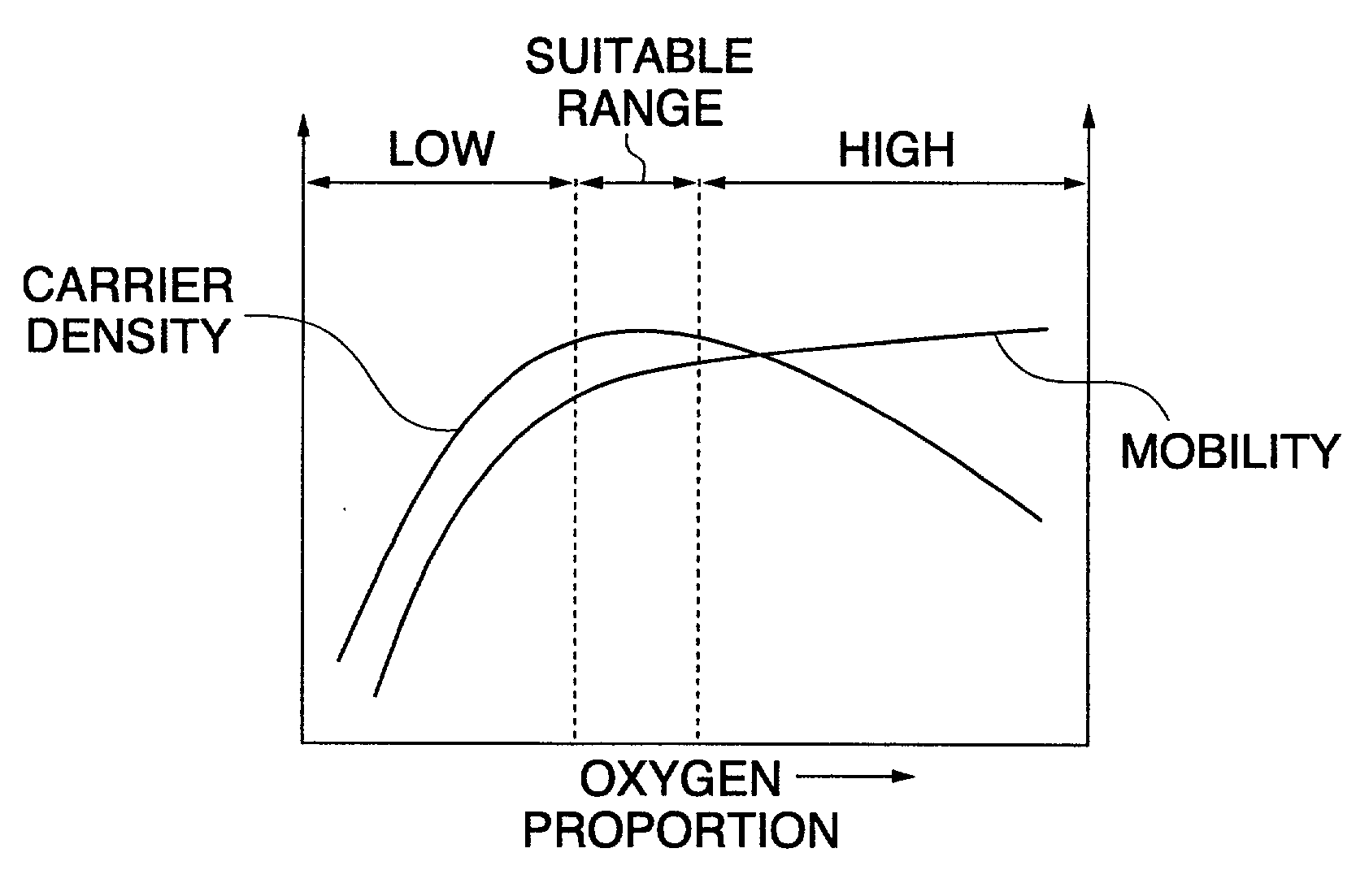
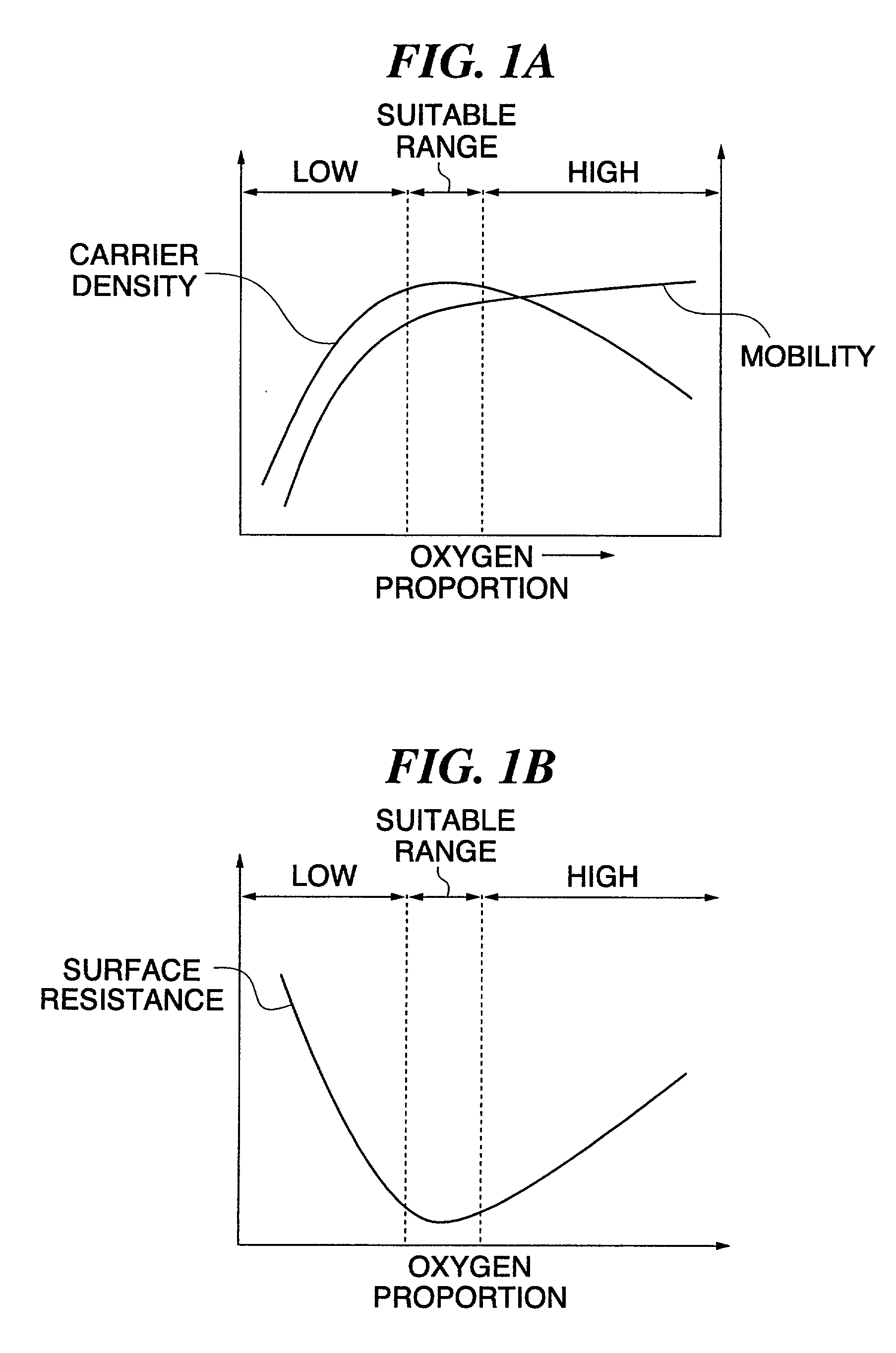
[0069] The following experiments were carried out to confirm the above findings.

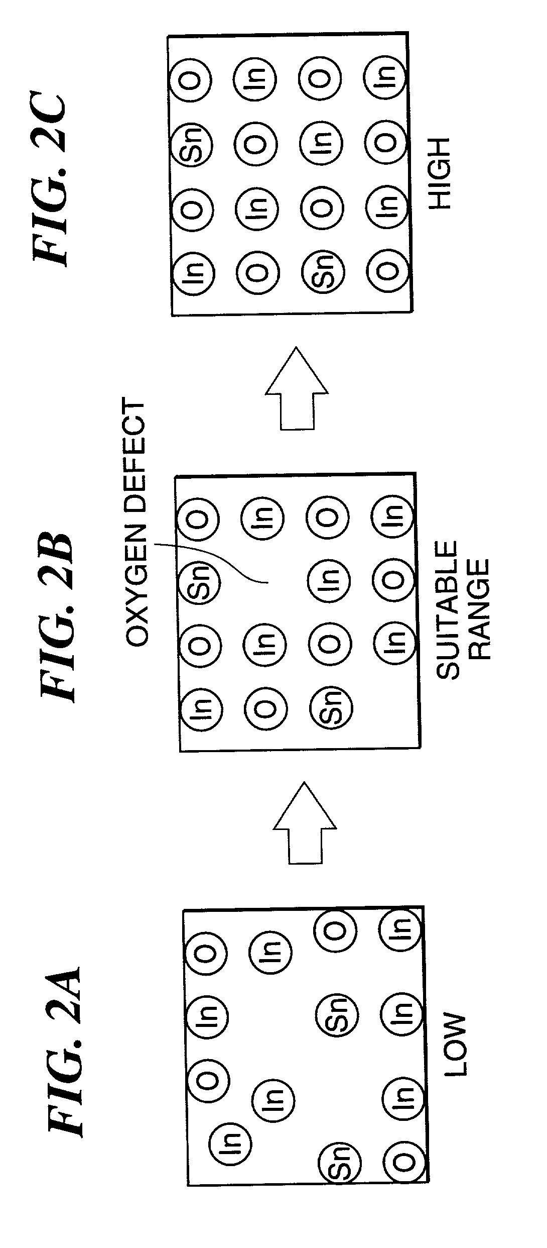
[0070] A soda lime glass substrate of size 300.times.400 mm and thickness 0.7 mm having an SiO.sub.2 film of thickness about 70 nm formed on both surfaces by liquid phase deposition was used. This substrate was cleaned with a neutral detergent in a dipping type ultrasonic cleaner, and then dried using a warm current of air. The cleaned substrate was then suspended from a jig specially designed for the purpose in a cylindrical rotating body of diameter 1700 mm and height 1260 mm placed in a chamber of internal diameter 1900 mm and height 2150 mm, and an ITO film was deposited by DC magnetron sputtering. The target used was an indium oxide / tin oxide target, with the amount of tin oxide added relative to the indium oxide being 10 mass %; two such targets of size 127 mm.times.914 mm were installed in the door part of the chamber.

[0071] 1000 cm.sup.3 per minute (under standard conditions) (hereinafter referre...


PUM

PropertyMeasurementUnit
thicknessaaaaaaaaaa
transmittanceaaaaaaaaaa
temperatureaaaaaaaaaa

Abstract

In a method of manufacturing a substrate having a transparent conductive film in which sputtering is carried out on a transparent insulating substrate using an indium oxide / tin oxide target under an atmosphere of a mixed gas containing argon and oxygen, when the ratio of oxygen to argon in the mixed gas is in a suitable range of 0.016 to 0.018, the carrier density of the transparent conductive film becomes a maximum, while the mobility rises progressively as the ratio of oxygen to argon increases. The surface resistance of the transparent conductive film, that is the reciprocal of the product of the carrier density and the mobility, 1 / (carrier densityxmobility), takes a minimum value when the ratio of oxygen to argon is in the above suitable range. In this case, crystallization of the film is promoted and the percentage change between the surface resistance of the film before heat treatment and the surface resistance of the film after heat treatment can be kept down to within ±10%.

Description

[0001] 1. Field of the Invention[0002] The present invention relates to a method of manufacturing a substrate having a transparent conductive film, a substrate having a transparent conductive film manufactured using the method, and a touch panel using the substrate.[0003] 2. Prior Art[0004] Conventionally, glass substrates having a tin-oxide-containing indium oxide (hereinafter referred to as `ITO`) film are widely used as the substrates having a transparent conductive film of liquid crystal display panels (hereinafter referred to as `LCDs`) and the like. In recent years, such glass substrates having an ITO film have also come to be used in resistive film type touch panels.[0005] As shown in FIG. 3, a resistive film type touch panel is composed of a transparent upper electrode 1 and a lower electrode 3, with the lower electrode 3 and the upper electrode 1 being arranged in facing relation to one another with spacers 2 therebetween; when the upper electrode 1 is pushed with a pen 4, ...

Claims


Application Information

Patent Timeline
Patent Type & Authority Applications(United States)
IPC IPC(8): C03C17/245C23C14/08C23C14/34G06F3/041G06F3/045H01B1/08H01B5/14H01B13/00H01H13/785
CPCC23C14/086G06F3/045H01B1/08H01H13/785H01H2201/028H01H2209/084C03C17/245
Inventor KIYOTA, SHOGOKATOH, YUKIHIRO
Owner NIPPON SHEET GLASS CO LTD
Why Eureka
Try Eureka