Apparatus and method for laser beam machining, and method for manufacturing semiconductor devices using laser beam machining

a laser beam machining and laser beam technology, applied in metal working apparatus, manufacturing tools, welding/soldering/cutting articles, etc., can solve the problems of poor exposure, drop in manufacturing yield, dust adhesion and accumulation on the processed area,

Inactive Publication Date: 2002-05-02
KK TOSHIBA
View PDF0 Cites 112 Cited by
  • Summary
  • Abstract
  • Description
  • Claims
  • Application Information

AI Technical Summary

Problems solved by technology

However, if laser beam machining is carried out in ordinary atmosphere, dust adheres to and accumulates on the processed areas.
Adhesion of the dust causes poor exposure, short-circuit, and breakdown, which further causes the manufacture yield to drop.
Moreover, since laser beam machining makes use of ablation (i.e., removal of materials as a result of melting and evaporation), the laser beam that illuminates the substrate or the laminated layers of metals (e.g., aluminum alloy, copper, etc.), insulators (SiO.sub.2, Si.sub.3N.sub.4, etc.), resins, etc. often causes damage to the irradiated regions and the area around them.
Similar damage is observed even if a KrF excimer laser or its analogues are used to process the silicon substrate in ordinary atmosphere.
Although machining lasers with a pulse width of several nanoseconds or greater, such as Q-swit

Method used


Image

  • Apparatus and method for laser beam machining, and method for manufacturing semiconductor devices using laser beam machining
  • Apparatus and method for laser beam machining, and method for manufacturing semiconductor devices using laser beam machining
  • Apparatus and method for laser beam machining, and method for manufacturing semiconductor devices using laser beam machining

Examples


first embodiment

[0049] (First Embodiment)

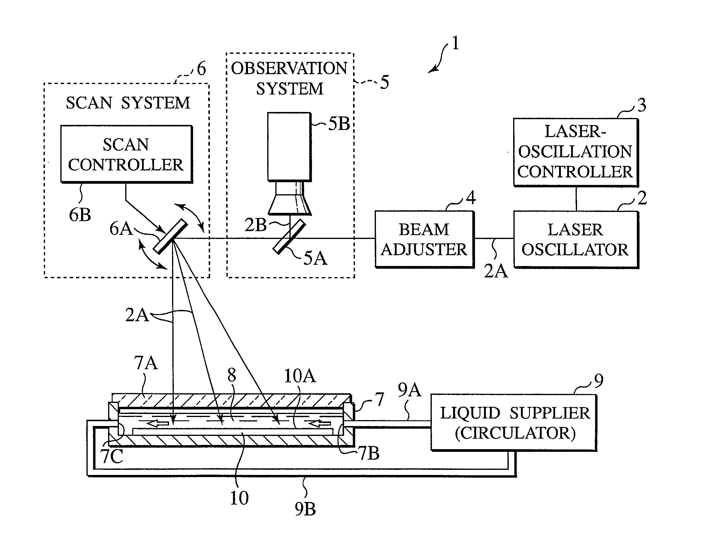
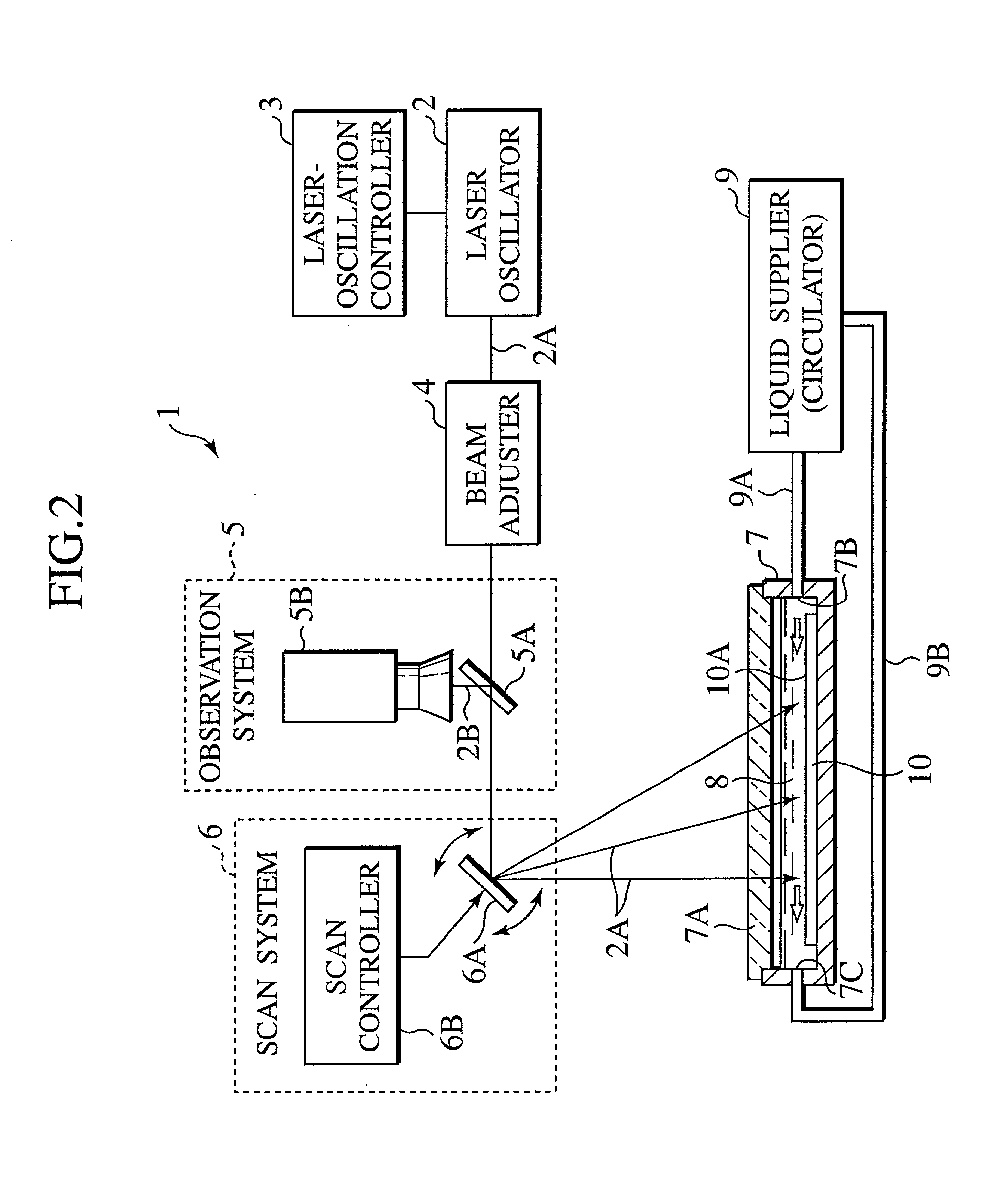
[0050] FIG. 2 illustrates a laser beam machining apparatus 1 according to the first embodiment of the invention. The laser beam machining apparatus 1 includes a laser oscillator 2, a holder 8 for holding an object 10 that is to be processed, a scanning system 6 for scanning the laser beam 2A emitted from the laser oscillator 2 on a target surface 10A of the object 10, and a liquid supplier 9 for supplying a liquid into the holder 6 (more particularly, to the target surface 10A). The holder 6 has an inlet port 7B and an outlet port 7C positioned so as to align with the target surface 10A of the object 10. In the following explanation, a silicon single crystal wafer 10 is used as an example of the object 10.

[0051] The laser beam machining apparatus 1 also includes a laser-oscillation controller 3, a beam adjuster 4, and an observation system 5 for observing the irradiation spot on the wafer 10.

[0052] The laser oscillator 2 is, for example, Q-switch Nd YAG lase...

second embodiment

[0067] (Second Embodiment)

[0068] FIG. 3 illustrates a laser beam machining apparatus 100 according to the second embodiment of the invention. The laser beam machining apparatus 100 comprises a laser oscillator 2, a holder 7 that holds the object to be processed (for example, a wafer) 10, a scanning system 6 for scanning a laser beam 2A emitted from the laser oscillator 2 on a target surface 10A of a wafer 10, a liquid supplier 9 for supplying a liquid 8 to the holder 7, and a ultrasonic application mechanism for providing a ultrasonic vibration to the target surface 10A of the wafer 10.

[0069] In the example of FIG. 3, the ultrasonic application mechanism is comprised of a piezoelectric element 120 attached to the rear face of the holder 7, and a driving controller 121 for controlling the motion of the piezoelectric element 120. Ultrasonic vibration propagates from the piezoelectric element 120 to the wafer 10 via the holder 7, and consequently, the target surface 10A of the wafer 10...

third embodiment

[0076] (Third Embodiment)

[0077] Various applications of the laser beam machining approach introduced in the first and second embodiments to a manufacturing process of semiconductor devices will now be described.

[0078] (1) Laser Beam Machining of a Semiconductor Substrate

[0079] FIG. 4 illustrates an example of forming a trench 11T in a semiconductor substrate (e.g., a silicon single crystal wafer) 11 using the laser beam machining approach of the first or second embodiment.

[0080] Laser beam machining is desired as an efficient dicing technique for cutting a wafer into chips, in place of a blade or a wire saw. As layers become thinner and thinner and the pattern on a semiconductor chip becomes finer and finer, a so-called first dicing technique is efficiently used to cut a semiconductor wafer into chips. With the first dicing technique, a groove that reaches halfway through the wafer is formed from the patterned surface of the wafer, and then, the wafer is polished from the bottom fac...


PUM

PropertyMeasurementUnit
Flow rateaaaaaaaaaa

Abstract

In a laser beam machining method, a liquid, through which a laser beam can be transmitted, is supplied to the target surface of an object to be processed. A laser beam is guided to the target surface through the liquid. The laser beam processes the target surface under the application of ultrasonic vibration.

Description

[0001] This patent application is based upon and claims the benefit of the earlier filing dates of Japanese Patent Application Nos. 2000-326361 and 2001-213671 filed Oct. 26, 2000 and Jul. 13, 2001, respectively, the entire contents of which are incorporated herein by reference.[0002] 1. Field of the Invention[0003] This invention relates to a technique of laser beam machining and a method for manufacturing semiconductor devices using the laser beam machining approach, and more substrates such as semiconductor wafers, glass substrates, or resin substrates, and thin films formed on these substrates.[0004] 2. Description of Related Art[0005] Since laser beam machining is capable of delineating fine patterns of an order of a micron (.mu.m) without requiring a lithography process, it has been attracting a great deal of attention as an approach to manufacturing semiconductor devices. In producing semiconductor devices, various types of layers, such as resist films, resin films, insulatin...

Claims


Application Information

Patent Timeline
IPC IPC(8): B23K26/12B23K26/16B23K26/36C23F1/18H01L21/268H01L21/306H01L21/3213
CPCB23K26/0732B23K26/0738B23K26/0807B23K26/121B23K26/16B23K26/365H01L21/76898B23K2201/40C23F1/18H01L21/268H01L21/30604H01L21/32131H01L21/32134B23K26/4075B23K26/40B23K26/082B23K26/1224B23K26/361B23K2101/40B23K2103/50
Inventor IKEGAMI, HIROSHIHAYASAKA, NOBUO
Owner KK TOSHIBA
Why Eureka
Try Eureka