Method of manufacturing semiconductor device

Inactive Publication Date: 2002-07-18
SEMICON ENERGY LAB CO LTD
View PDF7 Cites 41 Cited by
  • Summary
  • Abstract
  • Description
  • Claims
  • Application Information

AI Technical Summary

Problems solved by technology

It is difficult with a currently available technique to process a synthetic quartz glass substrate into a substrate having such a large area.
Even if that is possible, it is considered that its price cannot be reduced to a level practical for industrial use.
However, the distortion point temperature of Corning 7059 is 593.degree. C. and a problem is caused in the case of heating at 600.degree. C. or higher.
However, the heating time of 20 hours is too long for a mass production process.
However, according to the above technique, there is a problem in that the metallic element used for promoting crystallization is left also in high resistance layers (channel forming region and offset region).
Therefore, an off current is increased and thus variation between respective elements is produced, which causes deterioration in the stability and reliability

Method used


Image

  • Method of manufacturing semiconductor device
  • Method of manufacturing semiconductor device
  • Method of manufacturing semiconductor device

Examples


embodiment 1

[0088] [Embodiment 1]

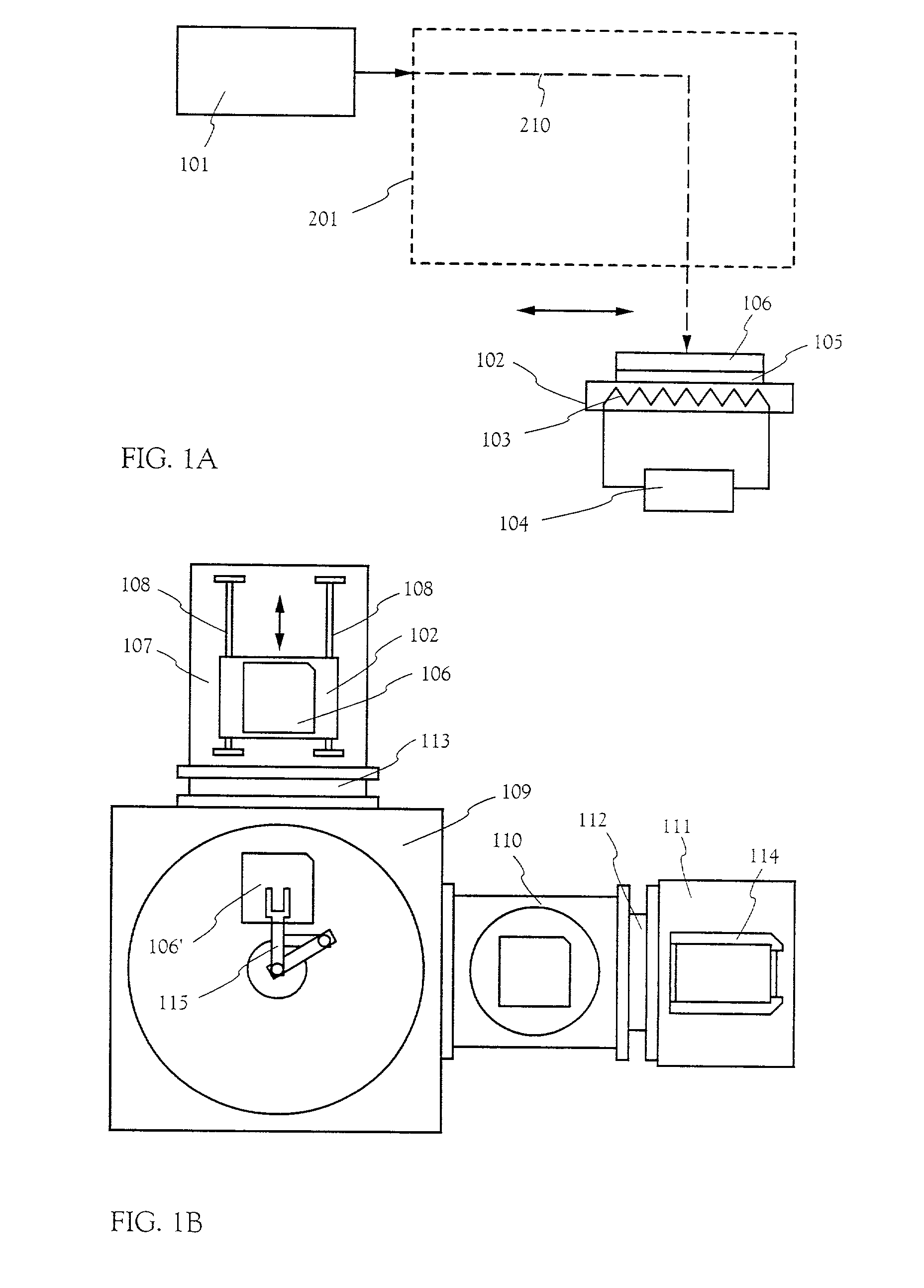
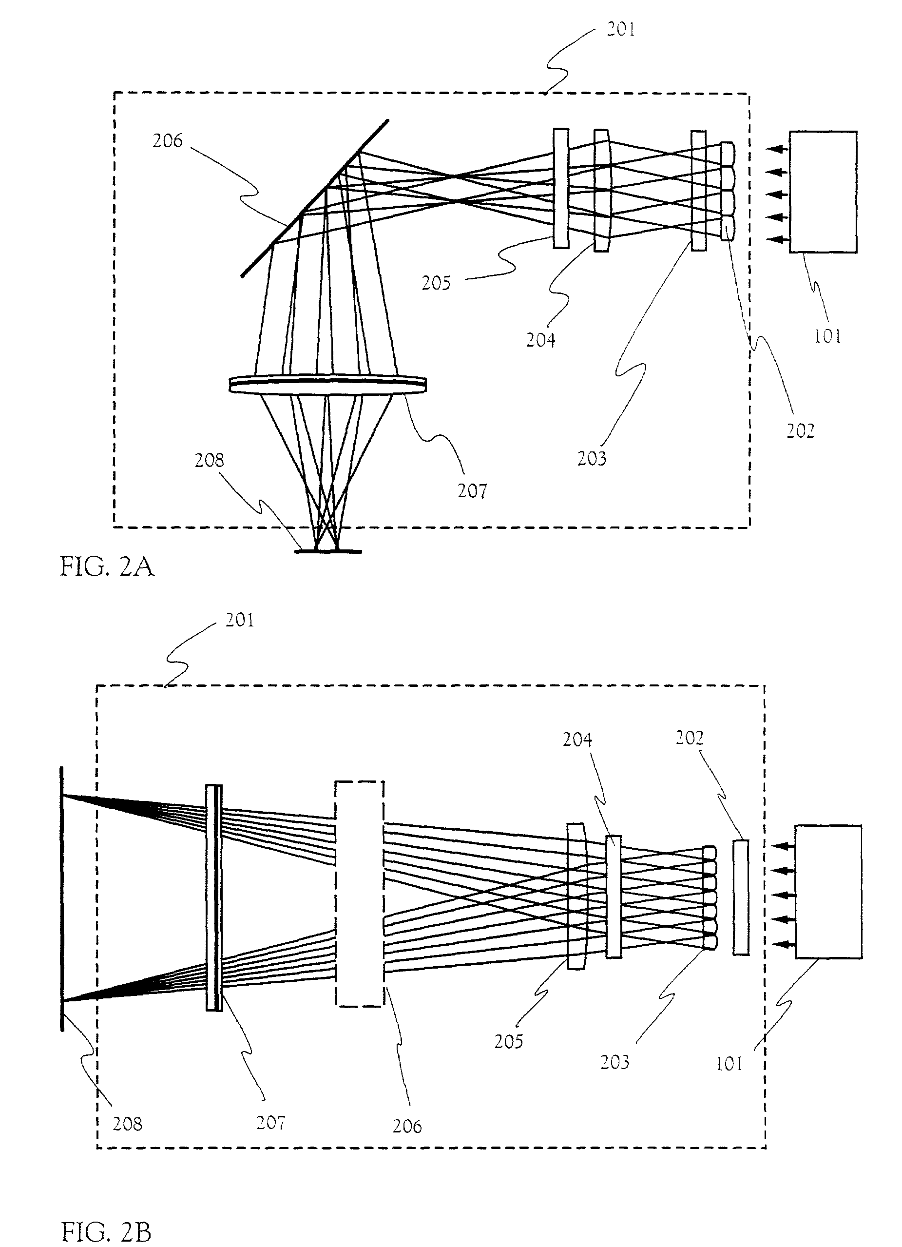
[0089] An embodiment of the present invention will be described. FIG. 1A shows a structure of a laser irradiation apparatus. This laser irradiation apparatus has a laser oscillator 101, an optical system 201 for linearly processing laser light 210 (preferably, the second harmonic) from the laser oscillator 101 as an oscillation source, and a stage 102 for holding a translucent substrate. A heater 103 and a heater controller 104 is provided in the stage 102 and thus the substrate can be heated at 100.degree. C. to 450.degree. C. Also, a reflector 105 is provided on the stage 102 and a substrate 106 on which a semiconductor film is formed is located thereon.

[0090] Note that, when the laser light outputted from the laser oscillator 101 is to he modulated to the second harmonic or the third harmonic, a wavelength modulator including a non-linear element may be provided immediately after the laser oscillator 101. In this embodiment, an Nd:YAG laser is used as the las...

embodiment 2

[0114] [Embodiment 2]

[0115] In this embodiment, the case where laser annealing is performed for a semiconductor film substrate obtained through manufacturing steps different from Embodiment 1 will be described.

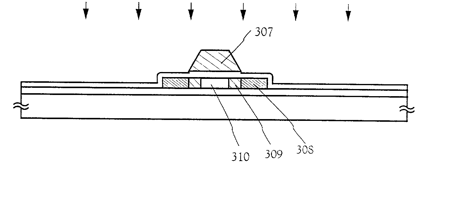
[0116] Here, a method of performing steps until the gate electrode of the TFT is formed will be described using FIGS. 7A to 7D. First, the state shown in FIG. 4A is obtained in accordance with Embodiment 1. Note that a state shown in FIG. 7A is the same state as in FIG. 4A.

[0117] Then, first thermal treatment is performed to crystallize a semiconductor film. Since the heating time and the heating temperature are dependent on the semiconductor film and the metallic element to be added, those are preferably determined as appropriate by an operator. In this embodiment, the semiconductor film is exposed at 550.degree. C. in an nitrogen atmosphere for 4 hours.

[0118] Successively, a mask 755 is formed and first doping processing is performed to selectively introduce an impurity elem...

embodiment 3

[0127] [Embodiment 3]

[0128] In this embodiment, the case where laser annealing is performed for a semiconductor film substrate obtained through manufacturing steps different from Embodiment 1 and Embodiment 2 will be described.

[0129] Here, a method of performing steps up to formation of the gate electrode of the TFT will be described using FIGS. 20A-20D. First, the state shown in FIG. 4A, in which a semiconductor film 302 is formed, is obtained in accordance with Embodiment 1. Note that the same reference numerals are used in FIG. 20A for the parts corresponding to those in FIG. 4A.

[0130] An insulating film including silicon such as a silicon oxide film or a silicon oxynitride film (SiOxNy) is formed as an insulating film 770 having an opening by a known process (sputtering method, LPCVD method, plasma CVD method, or the like). Then, a metallic element for promoting crystallization is added to form a metallic containing layer 771. Plasma processing, evaporation, a sputtering method,...


PUM

PropertyMeasurementUnit
Angleaaaaaaaaaa
Wavelengthaaaaaaaaaa
Temperatureaaaaaaaaaa

Abstract

The present invention is characterized in that gettering is performed such that impurity regions to which a noble gas element is added are formed in a semiconductor film and the metallic element included in the semiconductor film is segregated into the impurity regions by laser annealing. Also, a reflector is provided under a substrate on which a semiconductor film is formed. When laser light transmitted through the semiconductor film substrate is irradiated from the front side of the substrate, the laser beam is reflected by the reflector and thus the laser light can be irradiated to the semiconductor film from the read side thereof. Laser light can be also irradiated to low concentration impurity regions overlapped with a portion the gate electrode. Thus, an effective energy density in the semiconductor film is increased to thereby effect recovery of crystallinity and activation of the impurity element.

Description

[0001] 1. Field of the Invention[0002] The present invention relates to a semiconductor device manufactured by including the step of annealing a semiconductor film using a laser beam (hereinafter referred to as laser annealing) and a manufacturing method thereof. Note that the semiconductor device indicated here includes an electrooptical device such as a liquid crystal display device or a light emitting device and an electronic device including the electrooptical device as a part.[0003] 2. Description of the Related Art[0004] A technique for performing laser annealing to a semiconductor film formed on an insulating substrate made of glass or the like to crystallize it or to improve crystallininty thereof is widely studied. Silicon is often used for the above semiconductor film.[0005] Recently, in order to improve mass production efficiency, there is remarkable movement toward enlargement of a substrate such that the standard substrate size used in production lines of newly construc...

Claims


Application Information

Patent Timeline
IPC IPC(8): H01L21/00H01L21/268H01L21/322H01L21/336H01L21/77H01L21/84H01L27/12H01L29/786
CPCH01L21/268H01L21/3226H01L21/67103H01L21/67115H01L27/12H01L29/66757H01L29/66765H01L29/78621H01L29/78633H01L2029/7863H01L27/1285
Inventor YAMAZAKI, SHUNPEIMURAKAMI, SATOSHIOHNUMA, HIDETONAKAMURA, OSAMUTANAKA, KOICHIROARAI, YASUYUKI
Owner SEMICON ENERGY LAB CO LTD
Why Eureka
Try Eureka