Fabricating method of semiconductor integrated circuits

a technology of integrated circuits and fabrication methods, which is applied in the direction of semiconductor/solid-state device details, coatings, transistors, etc., can solve the problems of ruthenium film peeling, capacitors being poorly insulated, and not well conducted

Inactive Publication Date: 2002-08-01
RENESAS ELECTRONICS CORP
View PDF13 Cites 35 Cited by
  • Summary
  • Abstract
  • Description
  • Claims
  • Application Information

AI Technical Summary

Problems solved by technology

As a result, they are not well conducted.
However, even this process similarly causes the capacitor being poorly insulated.
Further, as a result of the transmission electron microscope (TEM) analysis, peeling due to shrinkage of the ruthenium film itself happens.
Consequently, it is conceivable that the capacitor is not well insulated because the bottom elect

Method used


Image

  • Fabricating method of semiconductor integrated circuits
  • Fabricating method of semiconductor integrated circuits
  • Fabricating method of semiconductor integrated circuits

Examples


embodiment 2

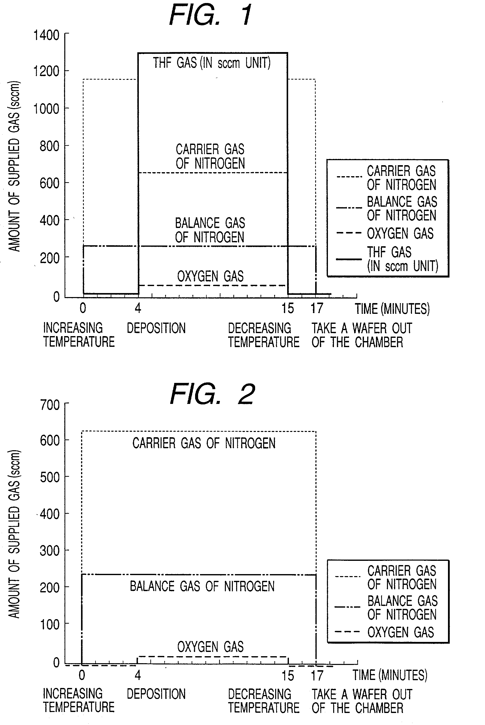
[0060] In this embodiment, a precursor gas, an oxidation gas, and an inert gas are introduced to form a bottom electrode of ruthenium. FIG. 7 shows the configuration of an apparatus. The case where a liquid precursor Ru(C.sub.5H.sub.4C.sub.2H.sub.5).sub.2 is loaded in a precursor container is taken as an example. Ru(C.sub.5H.sub.4C.sub.2H.sub.5).sub.2 is heated and vaporized by a vaporizer held at 150.degree. C., and carried by using a nitrogen gas as a carrier gas into a mixer. The flow rate is controlled by a mass flow controller (MFC). Then, the mixed gas is mixed with an oxygen gas, which is a reaction gas, before entering a deposition chamber. The precursor, oxygen gas, and the carrier gas of nitrogen are supplied through a distributor (shower-head) onto a wafer heated by a heater. The partial pressure of each gas in the deposition chamber is adjusted by making constant the flow rate of a balance gas of nitrogen supplied through another line and the total pressure in the deposi...

embodiment 3

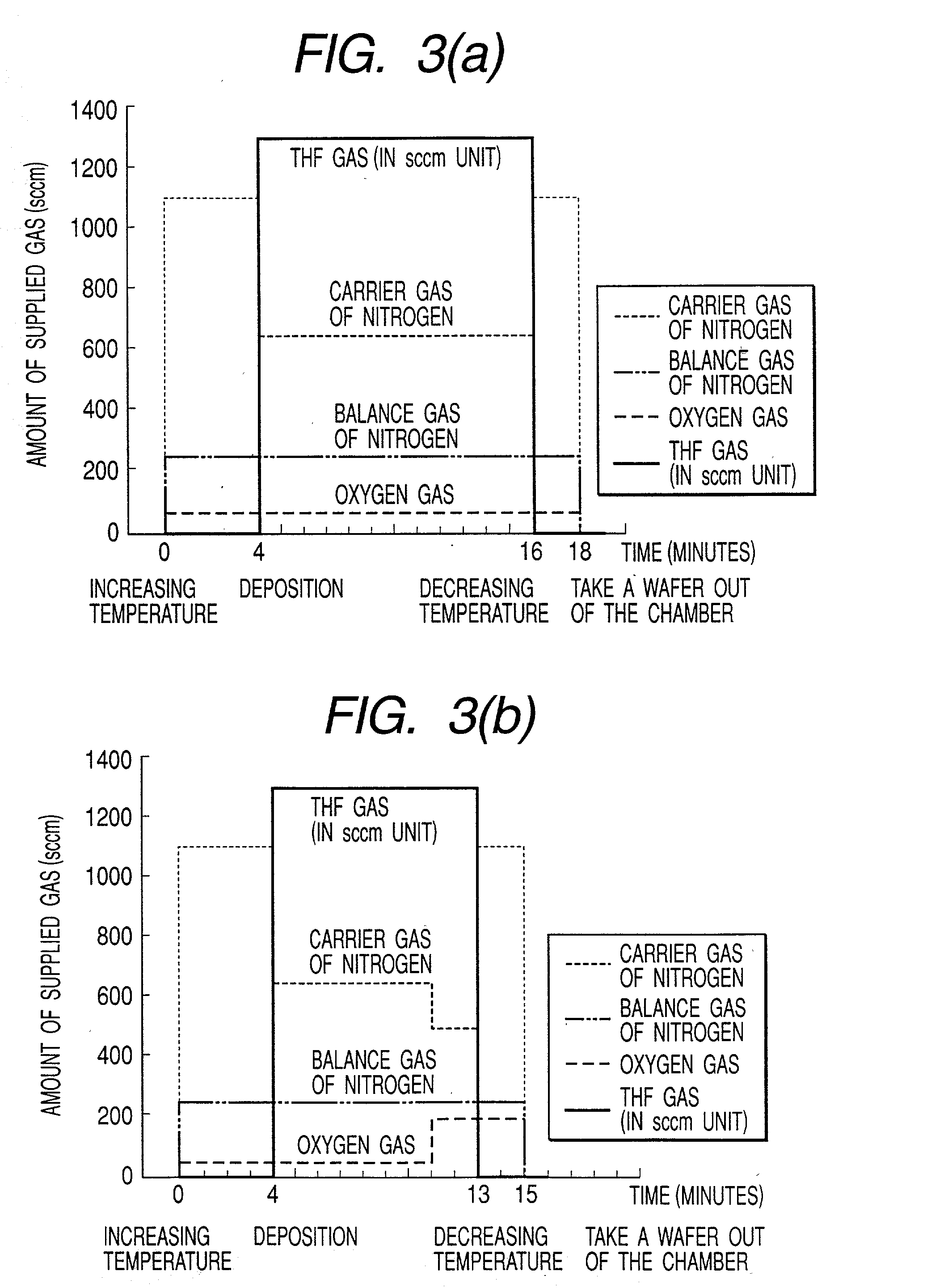
[0064] In this embodiment, a diluted precursor, a precursor gas, an oxidation gas, and an inert gas are introduce to form a top electrode of ruthenium. A diluted precursor of Ru(C.sub.5H.sub.4C.sub.2H.sub.5).sub.2 dissolved in a THF solvent with a concentration of 0.1 mol / l is used as a precursor. The apparatus configuration is the same as applied in Embodiment 1. When the top electrode of ruthenium is formed, an oxygen gas has to be supplied at both the times when increasing and decreasing the temperature of the wafer in order to inhibit an increase in the leakage current due to the reduction of the high-k dielectric film, such as a tantalum pentoxide film. The gas introduction process for forming the top electrode of ruthenium is as shown in FIG. 3(a).

[0065] A wafer is carried into the vacuum deposition chamber, and then the wafer temperature is increased up to 290.degree. C. over 4 minutes by a heater. At this step, the carrier gas of nitrogen and the balance gas of nitrogen are ...

embodiment 4

[0072] In this embodiment, a precursor gas, an oxidation gas, and an inert gas are introduced to form a top electrode of ruthenium. The apparatus configuration and the vaporization method of the precursor are shown in Embodiment 2. For example, if a liquid precursor Ru(C.sub.5H.sub.4C.sub.2-H.sub.5).sub.2 is loaded in a precursor container to form the top electrode of ruthenium, an oxygen gas has to be supplied at both the times when increasing and decreasing the temperature of the wafer in order to inhibit an increase in the leakage current due to the reduction of the high-k dielectric film, such as a tantalum pentoxide film. The gas introduction process is as shown in FIG. 4(a).

[0073] A wafer is carried into the vacuum deposition chamber, and then the wafer temperature is increased up to 250.degree. C. over 4 minutes by a heater. At this step, the carrier gas of nitrogen and the balance gas of nitrogen are supplied at rates of 600 sccm and 250 sccm, respectively. Further, an oxyge...


PUM

PropertyMeasurementUnit
Grain sizeaaaaaaaaaa
Partial pressureaaaaaaaaaa

Abstract

A ruthenium electrode with a low amount of oxygen contamination and high thermal stability is formed by a chemical vapor deposition method. In the chemical vapor deposition method using an organoruthenium compound as a precursor, the introduction of an oxidation gas is limited to when the precursor is supplying, and the reaction is allowed to occur at a low oxygen partial pressure. Consequently, it is possible to form a ruthenium film with a low amount of oxygen contamination. Further, after formation of the ruthenium film, annealing at not less than the formation temperature is performed, thereby forming a ruthenium film with high thermal stability.

Description

[0001] 1. Field of the Invention[0002] The present invention relates to a fabricating technology of a semiconductor integrated circuit. More particularly, it relates to a technology effectively adaptable for fabricating process a semiconductor integrated circuit with a step of forming a ruthenium electrode of a capacitor with high-k material by a chemical vapor deposition (CVD) method using an organoruthenium (Ru) compound as a precursor.[0003] 2. Description of the Related Art[0004] A DRAM (Dynamic Random Access Memory) is so configured that each one of its memory cells comprising a selective transistor and an information storage capacitor (below, referred to as a capacitor) are arranged in a matrix on a semiconductor substrate. The capacitance of the memory cell capacitor needs to be increased in density for configuring a large capacity DRAM. A method teaches using a tantalum pentoxide (Ta.sub.2O.sub.5) film with a high dielectric constant as a dielectric film of a capacitor in JP...

Claims


Application Information

Patent Timeline
IPC IPC(8): C23C16/18H01L21/02H01L21/28H01L21/285H01L21/3205H01L21/768H01L21/8242H01L23/52H01L27/108
CPCC23C16/18H01L21/28556H01L21/28568H01L28/55H01L28/60H01L28/91
Inventor SHIMAMOTO, YASUHIROHIRATANI, MASAHIKOMATSUI, YUICHIYAMAMOTO, SATOSHINABATAME, TOSHIHIDEANDO, TOSHIOSAKUMA, HIROSHIILJIMA, SHINPEI
Owner RENESAS ELECTRONICS CORP
Why Eureka
Try Eureka