Semiconductor material wet surface process passivation method

A semiconductor and wet process technology, applied in semiconductor/solid-state device manufacturing, electrical components, circuits, etc., can solve problems such as unfavorable subsequent application of III-V semiconductor materials, decreased passivation effect, and sodium ion pollution, and achieve enhanced passivation. Chemical stability, inhibition of oxidative corrosion, and reduction of volatilization of toxic gases

Inactive Publication Date: 2018-02-16
JILIN JIANZHU UNIVERSITY
View PDF5 Cites 2 Cited by
  • Summary
  • Abstract
  • Description
  • Claims
  • Application Information

AI Technical Summary

Problems solved by technology

At present, the reported sulfide passivation solutions mainly include NaS 9 h 2 O, (NH 4 ) 2 S, S 2 Cl, CH 3 CSNH 2 etc., but (NH 4 ) 2 S, S 2 Volatile H when passivated by Cl 2 S poisonous gas, NaS passivation has the problem of sodium ion pollution, and these sulfide passivations also have a prominent common disadvantage, that is, the sulfur p

Method used


Image

  • Semiconductor material wet surface process passivation method
  • Semiconductor material wet surface process passivation method

Examples


Embodiment Construction

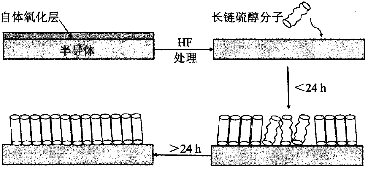
[0008] Step 1: Place the semiconductor wafer in acetone, ethanol, and deionized water for 5 to 10 minutes to ultrasonically clean it to remove organic contamination on the surface, and then rinse it with deionized water;

[0009] Step 2: Put the cleaned wafer into HF (HF:H 2 (O=1:1) soak in the solution for 3min to 10min to remove the thicker oxide layer on the wafer surface;

[0010] Step 3: Place the wafer in n-eicosanethiol (CH 3 [CH 2 ] 19 SH) in an ethanol solution, where the concentration of mercaptan is 5mM to 10mM, and the passivation is not less than 24h at room temperature;

[0011] Step 4: After the chip is taken out, put it into the isopropanol solution and sonicate it for not less than 5 minutes, and then dry it with high-purity nitrogen;

[0012] Step 5: The wafer is annealed under nitrogen condition, the temperature is 200±20°C, and the time is 30min±5min.


PUM


Abstract

The present invention relates to a semiconductor material wet surface process passivation method, belonging to the field of semiconductor material technology. Known technologies in the field are difficult to employ a wet process passivation means to maintain long-term stability of a passivation effect while effectively reducing a material surface state. A CH3[CH2]19SH is employed as a sulfide passivation solution and reacts with semiconductor materials in a special condition so that oxygen contamination at the surfaces of the semiconductor materials can be effectively removed, and a molecularlayer of a mercaptan with a long carbon chain is subjected to self-assembly at the surfaces of the semiconductor materials to realize stable passivation protection of the surfaces. The method providedby the invention is little in chemical pollution, simple to operate, low in cost and obvious in passivation effect, and can be used for surface process in a semiconductor device preparation process.

Description

technical field [0001] The invention designs a wet passivation method for the surface of a semiconductor material, in particular relates to a novel method for realizing stable passivation of the surface of a semiconductor material through an n-eicosanethiol solution, and belongs to the technical field of semiconductor materials. Background technique [0002] III-V semiconductor materials have the characteristics of large band gap, high electron mobility, direct band gap, high temperature resistance, etc., and become the most potential semiconductor material system after Si. They are used in semiconductor lasers, solar cells, MOS field effect transistors, Applications such as photodetectors have attracted attention. But due to lack of like Si / SiO 2 The stable passivation layer in the system and the high surface defect density of III-V semiconductor materials cause Fermi level pinning and high surface recombination rates, which directly affect the quality of the epitaxial lay...

Claims


Application Information

Patent Timeline
IPC IPC(8): H01L21/02
CPCH01L21/02112H01L21/02118H01L21/02282
Inventor 周路杨小天迟耀丹王欢初学峰闫兴振杨帆高晓红王超郭亮
Owner JILIN JIANZHU UNIVERSITY
Why Eureka
Try Eureka