Anisotropic conductive film

a conductive film and anisotropic technology, applied in the direction of non-metal conductors, connection contact materials, conductors, etc., can solve the problems of increased costs, waste of combination of a faulty electronic component and a good circuit board, and difficulty in fine pitch connection with the connection target, etc., to achieve good electrical continuity and low load

Inactive Publication Date: 2002-09-19
NITTO DENKO CORP
View PDF0 Cites 4 Cited by
  • Summary
  • Abstract
  • Description
  • Claims
  • Application Information

AI Technical Summary

Benefits of technology

[0009] In view of the above circumstances, it is a first object of the present invention to provide an anisotropic conductive film capable of ensuring good electrical continuity between an electronic component and a circuit board by thermal compression bonding at a low temperature at which the circuit board is not deteriorated. It is a second object of the present invention to provide an anisotropic conductive film wherein, in a functional test of an electronic component at a temperature of 150.degree. C. or higher, its film substrate does not adhere to the electronic component or a circuit board, the film ensures electrical continuity between the electronic component and the circuit board with a relatively low pressure (low load), and the film does not generate an out-gas.
[0010] With the aim of accomplishing the above objects, the present inventors conducted extensive investigations and found that a polycarbodiimide copolymer, wherein a polyalkylene carbonate unit is introduced to the polycarbodiimide molecule, is capable of softening or melting at relatively low temperatures without affecting the excellently low water absorption of a polycarbodiimide resin, that an anisotropic conductive film comprising a film substrate composed of this copolymer can adhere to both an electronic component and a circuit board at relatively low temperatures by thermal compression, that a thermal setting product of said copolymer possesses heat resistance to temperatures of 150.degree. C. or higher and is relatively flexible, and that an anisotropic conductive film comprising a film substrate composed of this thermal setting product is capable of ensuring electrical continuity between the electronic component and the circuit board simply by press adhering the film to the electronic component and the circuit board with a relatively low pressure (low load), thereby enabling testing of the both.

Problems solved by technology

However, this type of anisotropic conductive film poses structure-related problems, including difficulty in fine pitch connection with the connection target and necessity for a convex (bumpy) terminal of the connection target, e.g., electrode of semiconductor element.
An anisotropic conductive film is used as a testing connector to avoid poor yields and increased costs of circuit board, which occur when a functional test of an electronic component is conducted after mounting the electronic component on a circuit board, because a combination of a faulty electronic component and a good circuit board is wasted as being useless.
On the other hand, it has been found that a base substrate (resin substrate) of a circuit board of a semiconductor device (finished product with a semiconductor element mounted on the circuit board), obtained by thermal compression bonding at such a temperature is deteriorated and discolored, and causes connection failure between said semiconductor device and the mother board.
However, almost all the conventional anisotropic conductive films do not have heat resistance to endure high temperatures of 150.degree. C. or higher.
As a result, the film substrate may soften or melt, partly adhering to a circuit board (testing tool), and prevent continuous testing.
In other words, the circuit board may be no longer available for repeated use as a testing tool.
In a test using such an anisotropic conductive film at a temperature of 150.degree. C. or higher, however, gaseous silicon may be generated from the film substrate and contaminate the electronic component and / or the circuit board to prevent electrical continuity during the test, or the Si component may adhere to the electronic component (semiconductor element) and / or the circuit board to cause an error.

Method used


Image

  • Anisotropic conductive film
  • Anisotropic conductive film
  • Anisotropic conductive film

Examples


first embodiment

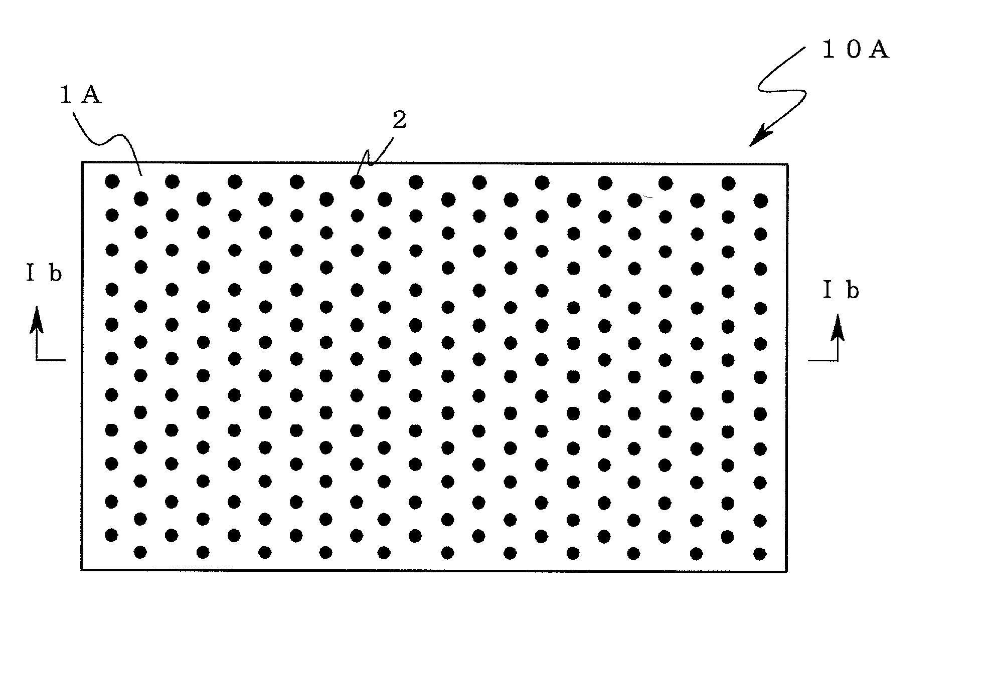
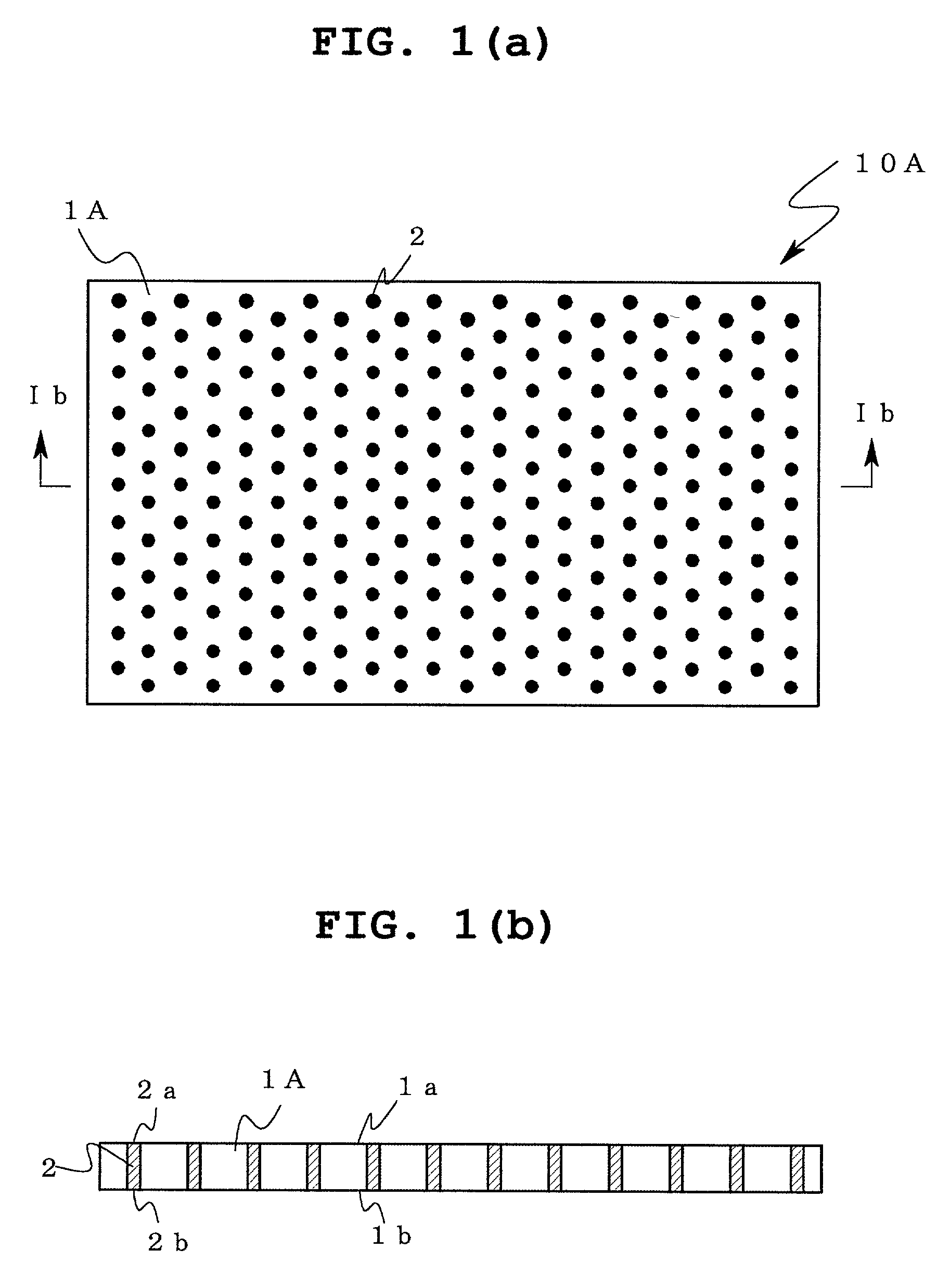
[0036] As described above, when a conventional anisotropic conductive film employing a polycarbodiimide resin for the film substrate 1A is used as a mounting connector, connection targets (electronic component and circuit board) cannot be connected satisfactorily (joined firmly to provide electrical continuity) unless the anisotropic conductive film is heated to a temperature of 250.degree. C. or higher for thermal compression bonding. On the other hand, when the anisotropic conductive film of the present invention is used, the film substrate 1A softens or melts sufficiently upon heating at a low temperature of about 150 to 200.degree. C. so that a good connection can be achieved between said film and the subjects of connection. In addition, because the film substrate 1A possesses favorably low water absorption derived from the polycarbodiimide resin, the finished product obtained by mounting (e.g., a semiconductor device wherein a semiconductor element is mounted on a circuit board...

second embodiment

[0069] The anisotropic conductive film of the present invention is hereinafter described.

[0070] FIG. 4 shows an example of the anisotropic conductive film of the second embodiment of the present invention, i.e., an anisotropic conductive film especially useful as a testing connector. FIG. 4(a) is a plan view, and FIG. 4(b) is a cross-sectional view along the line IVb-IVb in FIG. 4(a). The anisotropic conductive film of the second embodiment of the present invention, as represented by this anisotropic conductive film 10B in FIG. 4, has a plurality of conductive paths 2 insulated from each other in the film substrate 1B comprising an insulating resin and penetrating the film substrate 1B in the direction of the thickness of the film substrate 1B, both ends 2a and 2b of each conductive path 2 being exposed to the top and back faces 1a and 1b, respectively, of the film substrate 1B, wherein the film substrate 1B is mainly composed of a setting product of the polycarbodiimide copolymer o...

example 1

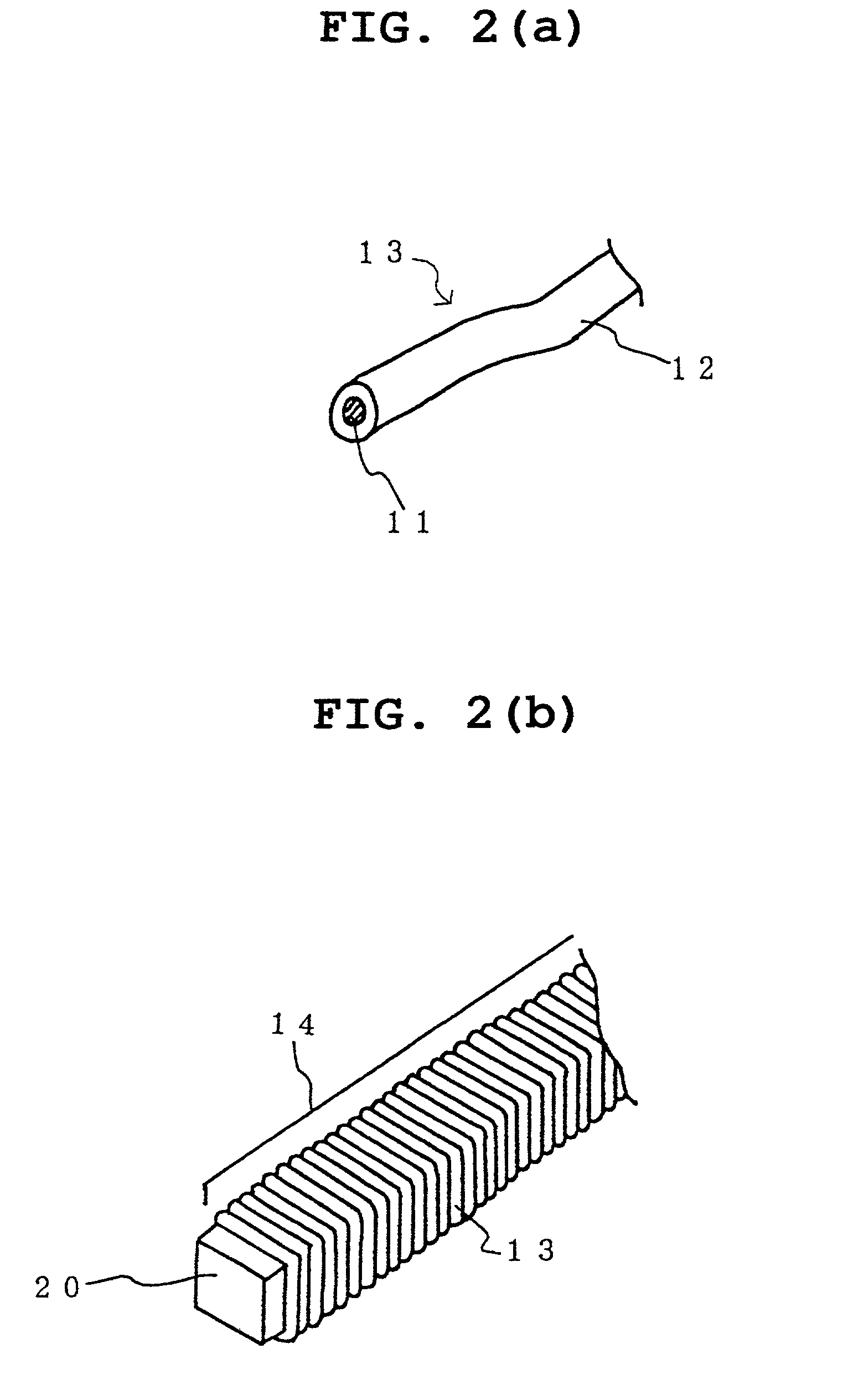
[0088] A mixture (100 g) of tolylene diisocyanate (2,4-tolylene diisocyanate (2,4-TDI) and 2,6-tolylene diisocyanate (2,6-TDI) (2,4-TDI:2,6-TDI=2:8 (molar ratio)) and polyhexamethylene carbonate diol (100 g) were urethanized by a reaction in a mixed solvent (100 g) of xylene and cyclohexane at 100.degree. C. for 3 hours. Subsequently, 3-methyl-1-phenyl-2-phosphorene-1-oxide (0.883 g) and p-isopropylphenyl isocyanate (6.47993 g) were added, and this was followed by polymerization at 100.degree. C. for 1 hour to yield a solution of a polycarbodiimide copolymer resulting from copolymerization of polyhexamethylene carbonate. This solution was dried at 90.degree. C. for 30 minutes and at 200.degree. C. for 30 minutes to yield a film, and the polycarbodiimide copolymer was collected as a solid. The glass transition temperature of this solid was determined to be 130.degree. C. The number-average molecular weight of this solid was determined to be 6300.

[0089] An insulated lead wire was prep...


PUM

PropertyMeasurementUnit
glass transition temperatureaaaaaaaaaa
elastic modulusaaaaaaaaaa

Abstract

As an anisotropic conductive film capable of firmly adhering to an electronic component and a circuit board and achieving good electrical continuity by thermal compression bonding at a low temperature at which the circuit board is not deteriorated, an anisotropic conductive film is provided, which has a plurality of conductive paths 2 insulated from each other and penetrating the film substrate 1A in the direction of the thickness of the film substrate, both ends 2a and 2b of each conductive path being exposed to the top and back faces of the film substrate, wherein the film substrate 1A is mainly composed of a polycarbodiimide copolymer having a structure represented by formula (I) below: R.sub.3--NCNR.sub.2--NCN.paren close-st..sub.nR.sub.2--AR.sub.1--O--CO--O.- paren close-st..sub.mR.sub.1--A--R.sub.2.sub.xNCN--R.sub.2.paren close-st..sub.nNCN--R.sub.3 (I) wherein m represents an integer of 2-50; n represents an integer of 1-30; x represents an integer of 1-10; A represents a urethane bond; R.sub.1 represents an alkylene group; R.sub.2 represents an aromatic diisocyanate residue; and R.sub.3 represents an aromatic monoisocyanate residue.

Description

FIELD OF THE INVENTION[0001] The present invention relates to an anisotropic conductive film, and more specifically to an anisotropic conductive film comprising a polycarbodiimide copolymer as a material of a film substrate.BACKGROUND OF THE INVENTION[0002] In recent years, anisotropic conductive films have been widely used as connector materials to electrically connect electronic components, such as a semiconductor element (IC chip), and circuit boards.[0003] Conventionally-known anisotropic conductive films are formed by dispersing conductive microparticles in a film substrate made of an insulating resin. However, this type of anisotropic conductive film poses structure-related problems, including difficulty in fine pitch connection with the connection target and necessity for a convex (bumpy) terminal of the connection target, e.g., electrode of semiconductor element. Accordingly, W098 / 07216 proposes an anisotropic conductive film having a plurality of conductive paths insulated ...

Claims


Application Information

Patent Timeline
Patent Type & Authority Applications(United States)
IPC IPC(8): C08G18/02C08J5/18C09J179/00H01B1/12H01B5/16H01L21/60H01R11/01H05K3/32
CPCH01B1/12H01L24/83H01L2224/8319H01L2224/838H01L2924/01004H01L2924/01005H01L2924/01013H01L2924/01015H01L2924/01025H01L2924/01027H01L2924/01029H01L2924/01033H01L2924/0105H01L2924/01078H01L2924/01079H01L2924/01082H01L2924/01327H01L2924/0781H01L2924/14H01L24/29H01L2224/2919H01L2224/29298H01L2224/83101H01L2924/01006H01L2924/01019H01L2924/01024H01L2924/01087H01L2924/014H01L2924/0665H01L2224/29101H01L2924/00H01L2924/00011H01L2924/3512H01L2224/29199H01L2924/00013H01L2224/29299H01L2224/2929H01L2224/29099C08J5/18
Inventor YAMAGUCHI, MIHOMISUMI, SADAHITOHOTTA, YUJI
Owner NITTO DENKO CORP
Why Eureka
Try Eureka