Mask-making member and its production method, mask and its making method, exposure process, and fabrication method of semiconductor device

a mask-making member and production method technology, applied in the direction of semiconductor/solid-state device details, optical radiation measurement, therapy, etc., can solve the inconvenience of circuit pattern inability to accurately transfer circuit patterns by exposure, low throughput of block full exposure system, and low throughput. achieve the effect of high accuracy and low cos

Inactive Publication Date: 2002-09-19
SONY CORP
View PDF11 Cites 23 Cited by
  • Summary
  • Abstract
  • Description
  • Claims
  • Application Information

AI Technical Summary

Benefits of technology

[0007] An object of the present invention is to provide a mask-making member capable of highly accurately making a mask for a charged particle beam reduction-and-division transfer exposure system at a low cost and a method of producing the mask-making member, a mask made from the mask-making member and a method of making the mask made from the mask-making member, an exposure process using the mask, and a method of fabricating a semiconductor device using the mask.
[0008] The present inventor has earnestly examined to solve the above-described problems of the related art electron beam exposure systems, and found that the following two measures are effective to solve the above problems.
[0057] According to the inventions configured as described above, since the first alignment marks are formed by exposure at a time in the supporting region of the mask-making member and exposure of the mask for forming the mask circuit patterns thereon is performed by using the first alignment marks, the positional accuracy of the whole of the mask circuit patterns due to the first alignment marks can be significantly enhanced. Further, the distance between two of the first alignment marks on one mask is not different from that on another mask, so that a mask exposure system used for exposure of the mask for forming the mask circuit patterns thereon may have only a performance capable of forming the mask circuit patterns in small regions by using the first alignment marks. In other words, an expensive mask exposure system using light having a low throughput is not required to be used as the mask exposure system for exposure of the mask for forming the mask circuit patterns thereon.
[0059] Even by using an exposure system not allowed to form all of the alignment marks on the mask by exposure at a time, for example, a reduction transfer exposure system using light, the mask circuit patterns can be highly accurately formed by using the alignment marks for exposure of a mask.
[0060] According to the inventions described above, a deviation and a distortion of an electron-optical system and a stage mechanism system of a charged particle beam reduction-and-division transfer exposure system can be corrected by dividedly transferring a positional deviation measurement pattern on a test mask onto a substrate at a specific reduction ratio by means of exposure of the substrate by the charged particle beam reduction-and-division transfer exposure system using the test mask, and detecting the deviation and the distortion of the electron-optical system and the stage mechanism system of the exposure system on the basis of the transferred positional deviation pattern. Accordingly, it is possible to perform exposure of the mask for forming the mask circuit patterns thereon while correcting the deviation and distortion.
[0061] According to the inventions described above, since the same master mask is used for forming alignment marks on each of a plurality of masks used in a plurality of exposure steps in the method of fabricating a semiconductor device, it is possible to improve the overlapped accuracy between layers upon exposure of a semiconductor substrate.

Problems solved by technology

An electron beam exposure process is effective to form finer circuit patterns; however, it has a disadvantage that a throughput (amount treated per unit time) is low.
In the case of forming the recent highly integrated circuit patterns by exposure, however, this block full exposure system is yet significantly low in throughput than the existing exposure system using light.
In this electron beam reduction transfer exposure system, however, if the entire mask equivalent to the whole of the integrated circuit chip is full irradiated with electron beams, there may occurs an inconvenience that the circuit pattern cannot accurately transferred by exposure.
If a mask exposure system for making a mask, which mask is used for the electron beam reduction-and-division transfer exposure system of a reduction ratio of {fraction (1 / 4)}, is required to have a performance comparable to that required for the corresponding mask exposure system using light, a significantly expensive mask exposure system must be used as the above mask exposure system for making a mask by using electron beams.
Further, to attain highly accurately exposure over the entire surface of a mask, various kinds of correction are required to be performed during exposure, resulting in the degraded throughput.
This method, however, has problems that a throughput is low, and that a pattern forming system excellent in long-dimension accuracy has been not obtained yet at the present time.
Another problem of the electron beam reduction-and-division transfer exposure system is as follows: namely, although any exposure system is designed to transfer a circuit pattern formed on a mask onto a substrate as accurately as possible, there may occur a slight deviation in transfer between one and another of the exposure systems depending on assembling accuracy of each of the exposure systems.
An electron beam direct wiring type exposure system such as a variable shaped beam exposure system or a block full exposure system can correct such a deviation at any time by adjusting an electron-optical system while monitoring a condition of the exposure system; however, the transfer exposure system is difficult to correct an electron-optical system at any time because it transfers a circuit pattern on a mask on a substrate at a time.

Method used


Image

  • Mask-making member and its production method, mask and its making method, exposure process, and fabrication method of semiconductor device
  • Mask-making member and its production method, mask and its making method, exposure process, and fabrication method of semiconductor device
  • Mask-making member and its production method, mask and its making method, exposure process, and fabrication method of semiconductor device

Examples


first embodiment

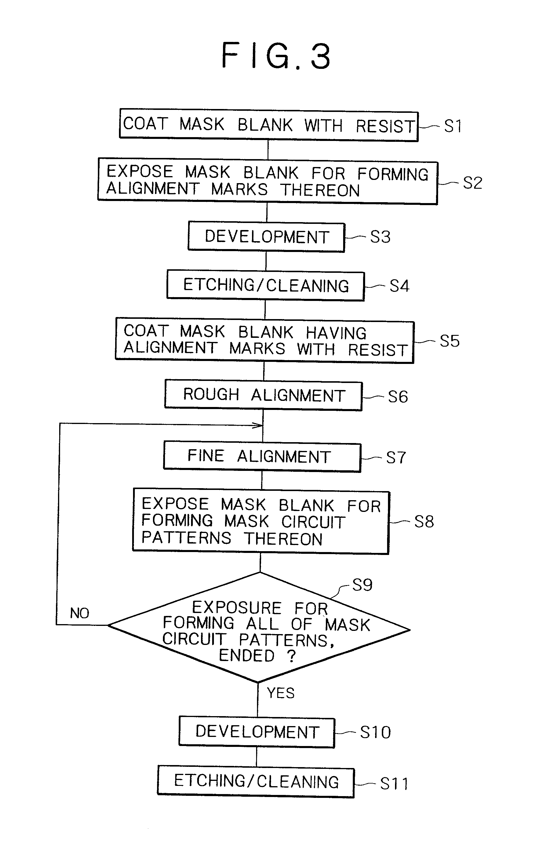
[0083] FIG. 3 is a flow chart showing a method of making a mask according to the present invention.

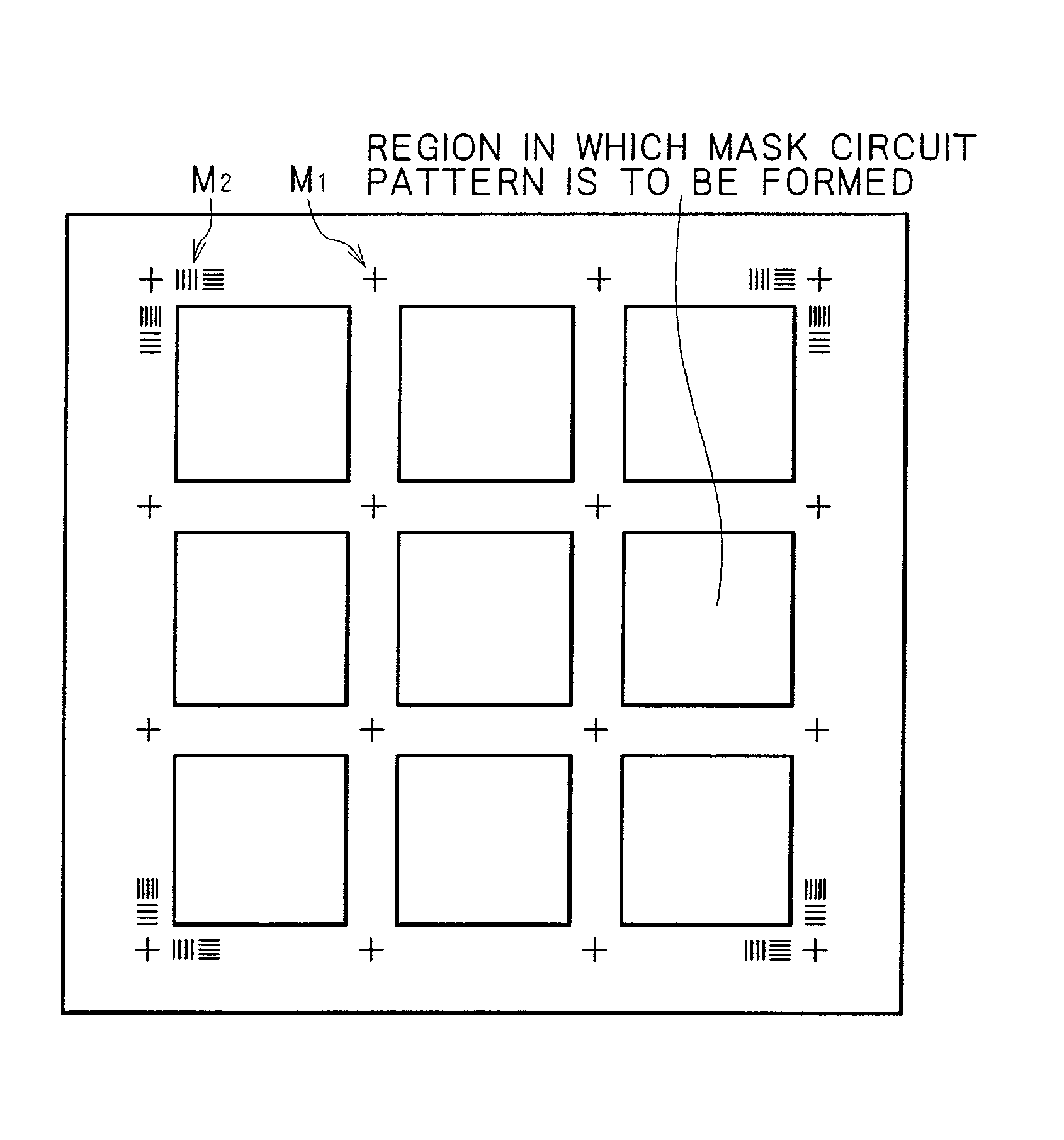
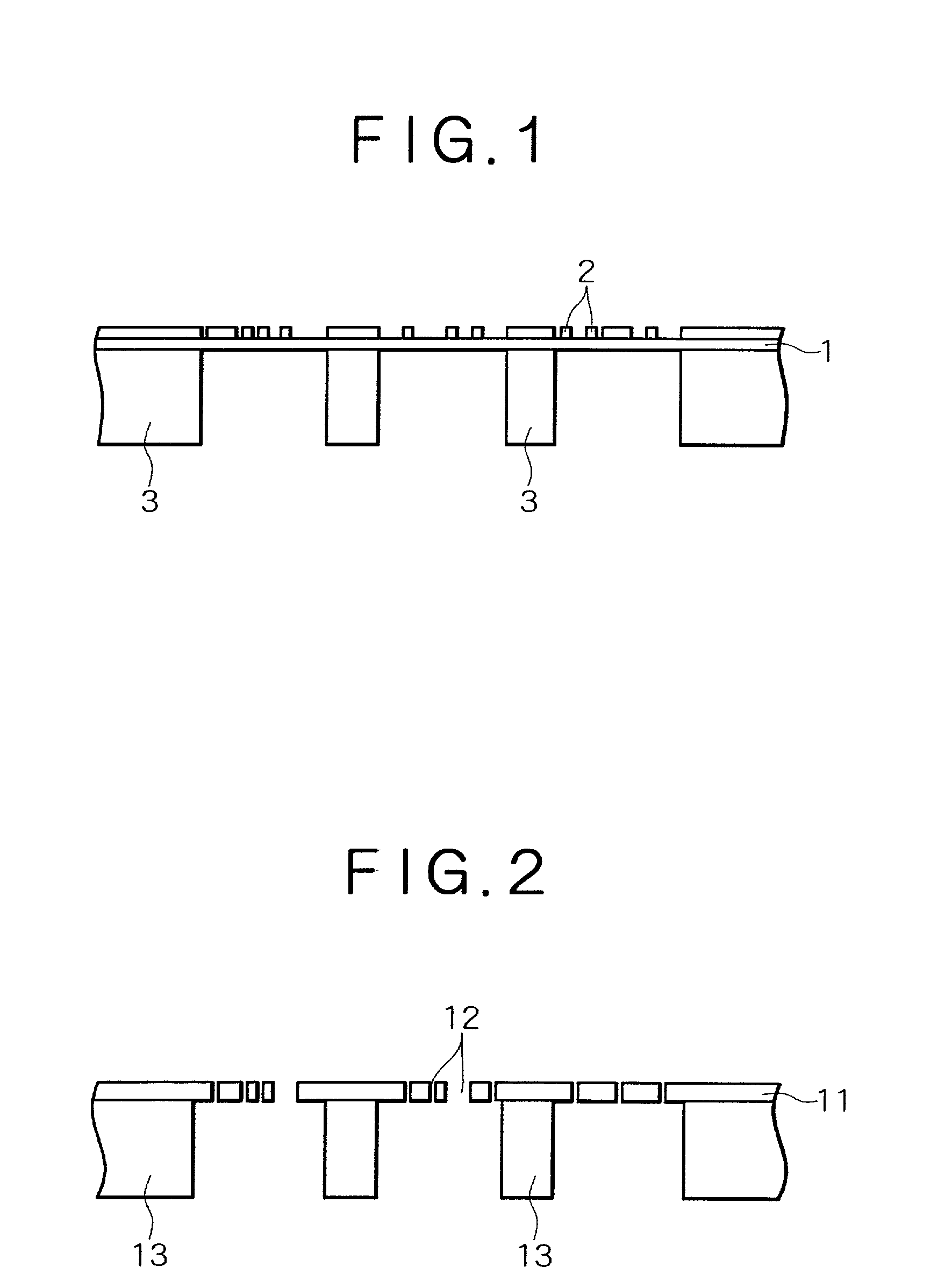
[0084] As shown in FIG. 3, according to the first embodiment, a mask blank is coated with a resist in step S1. FIGS. 4A to 4C show a mask blank for a mask which is used in an electron beam reduction-and-division transfer exposure system, wherein FIG. 4A is a top view of the mask blank from which the membrane 1 provided with the electron scatterer 2 or the mask board 11 is omitted, FIG. 4B is a sectional view of the mask blank configured as a transmission mask, and FIG. 4C is a sectional view of the mask blank configured as a stencil mask. In the mask blank shown in FIGS. 4A to 4C, as described above, mask circuit patterns are to be formed on the small regions separated from each other by means of the supports 3 or 13. Each of the small regions is formed into a square shape typically having one side of about 1 mm, and each of the supports 3 or 13, which constitute a supporting region am...

third embodiment

[0099] the present invention will be described below. FIG. 9 shows a concept of correction for a positional deviation of an electron beam reduction-and-division transfer exposure system by using a test mask, and FIG. 10 shows a flow chart illustrating the correction for a positional deviation by using the test mask.

[0100] According to the third embodiment, a test mask is first prepared in step S101. FIGS. 11, 12 and 13 show examples of test patterns transferred on a substrate such as a wafer. In the case of evaluating only stitching accuracies of circuit patterns dividedly transferred, the test patterns shown in FIGS. 11 and 12 may be used.

[0101] FIG. 11 shows a test pattern used in the case where two character pattern portions to be dividedly transferred by exposure are not overlapped to each other at a boundary between the two pattern portions. In this case, a deviation of a relative positional relationship between the two character pattern portions, opposed to each other with the...


PUM

PropertyMeasurementUnit
sizeaaaaaaaaaa
sizeaaaaaaaaaa
thicknessaaaaaaaaaa

Abstract

A mask blank has a plurality of pattern formation regions in which mask circuit patterns are to be formed, and a supporting region in which any mask circuit pattern is not to be formed. The supporting region is provided for holding the plurality of pattern formation regions while separating the plurality of pattern formation regions from each other. The supporting region has first and second alignment marks. Exposure of a mask made from the mask blank for forming mask circuit patterns thereon is performed on the basis of the first alignment marks, and exposure of a substrate for forming circuit patterns thereon is performed on the basis of the second alignment marks. With this configuration, a mask used for charged particle beam reduction-and-division transfer exposure can be highly accurately produced at a low cost, and exposure of a substrate can be highly accurately performed by using the mask.

Description

BACKGROUND OF THE INVENTION[0001] The present invention relates to a member for making a mask and a method of producing the mask-making member, a mask made from the mask-making member and a method of making the mask made from the mask-making member, an exposure process using the mask, and a method of fabricating a semiconductor device using the mask. In particular, the present invention relates to a technique suitable for exposure of a substrate such as a wafer to charged particle beams, typically, electron beams.[0002] Semiconductor integrated circuit devices, liquid crystal display units, CCD devices, and the like have been fabricated by using a fine processing technique for semiconductors. Along with the increased degree of integration of these semiconductor devices, circuit patterns formed thereon have become finer, and to form such finer circuit patterns, exposure by charged particle beams, particularly, electron beams have become a focus of attention. An electron beam exposure...

Claims


Application Information

Patent Timeline
Patent Type & Authority Applications(United States)
IPC IPC(8): G03F1/20G03F7/20G03F9/00H01J37/305H01L21/027H01L23/544
CPCG03F1/20H01J2237/0435H01J2237/31791H01L23/544H01L2223/5442H01L2223/54453Y10S438/975H01L2924/0002H01L2924/00
Inventor KOIKE, KAORUMORIYA, SHIGERU
Owner SONY CORP
Why Eureka
Try Eureka