
Inspection method and inspection apparatus

a technology of inspection apparatus and inspection method, which is applied in the direction of electronic circuit testing, measurement devices, instruments, etc., can solve the problems of difficult detection of each defective spot, difficult to identify patterns, and complicated inspection steps

Inactive Publication Date: 2002-09-19
SEMICON ENERGY LAB CO LTD
View PDF5 Cites 57 Cited by
  • Summary
  • Abstract
  • Description
  • Claims
  • Application Information

AI Technical Summary

Benefits of technology

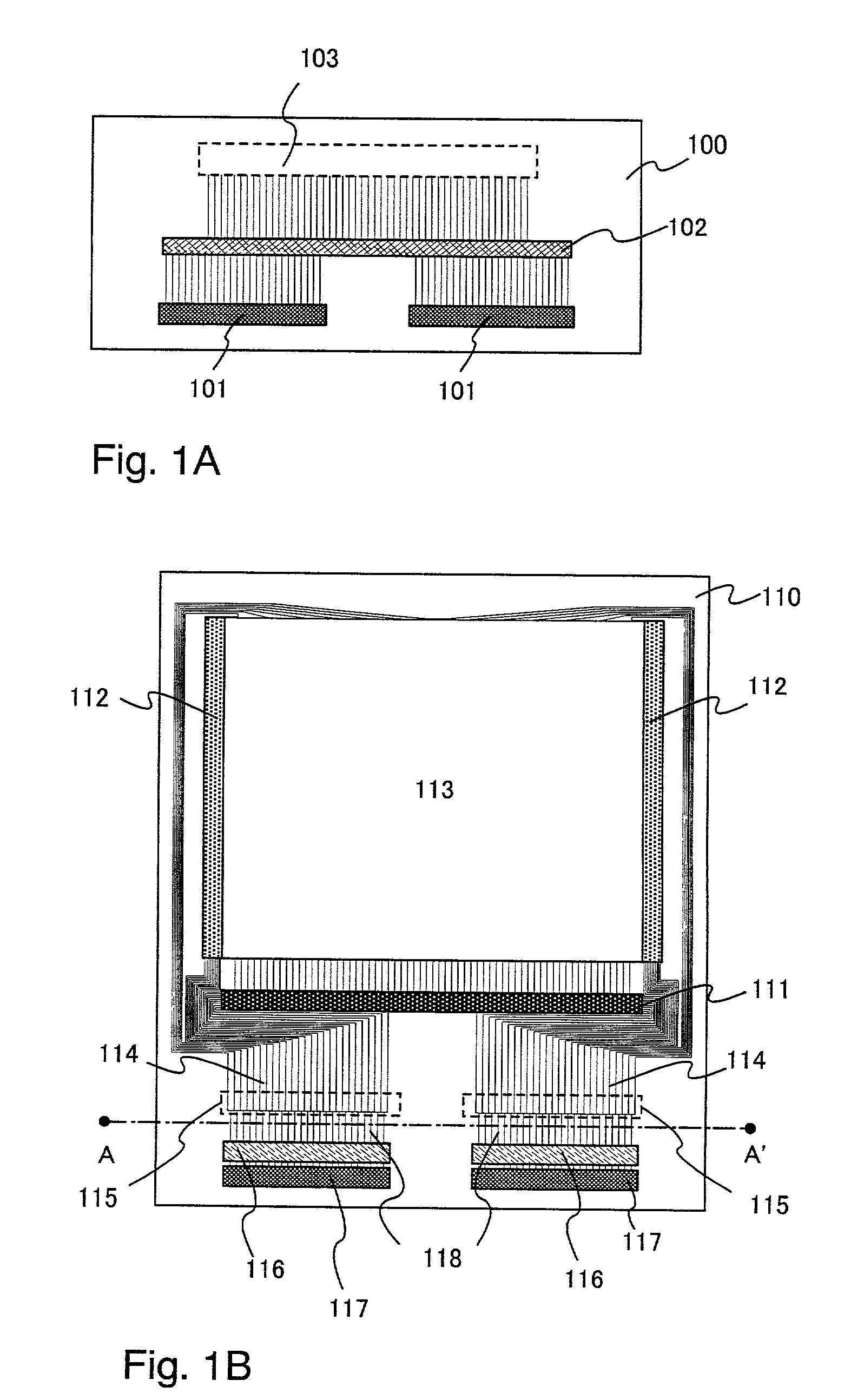
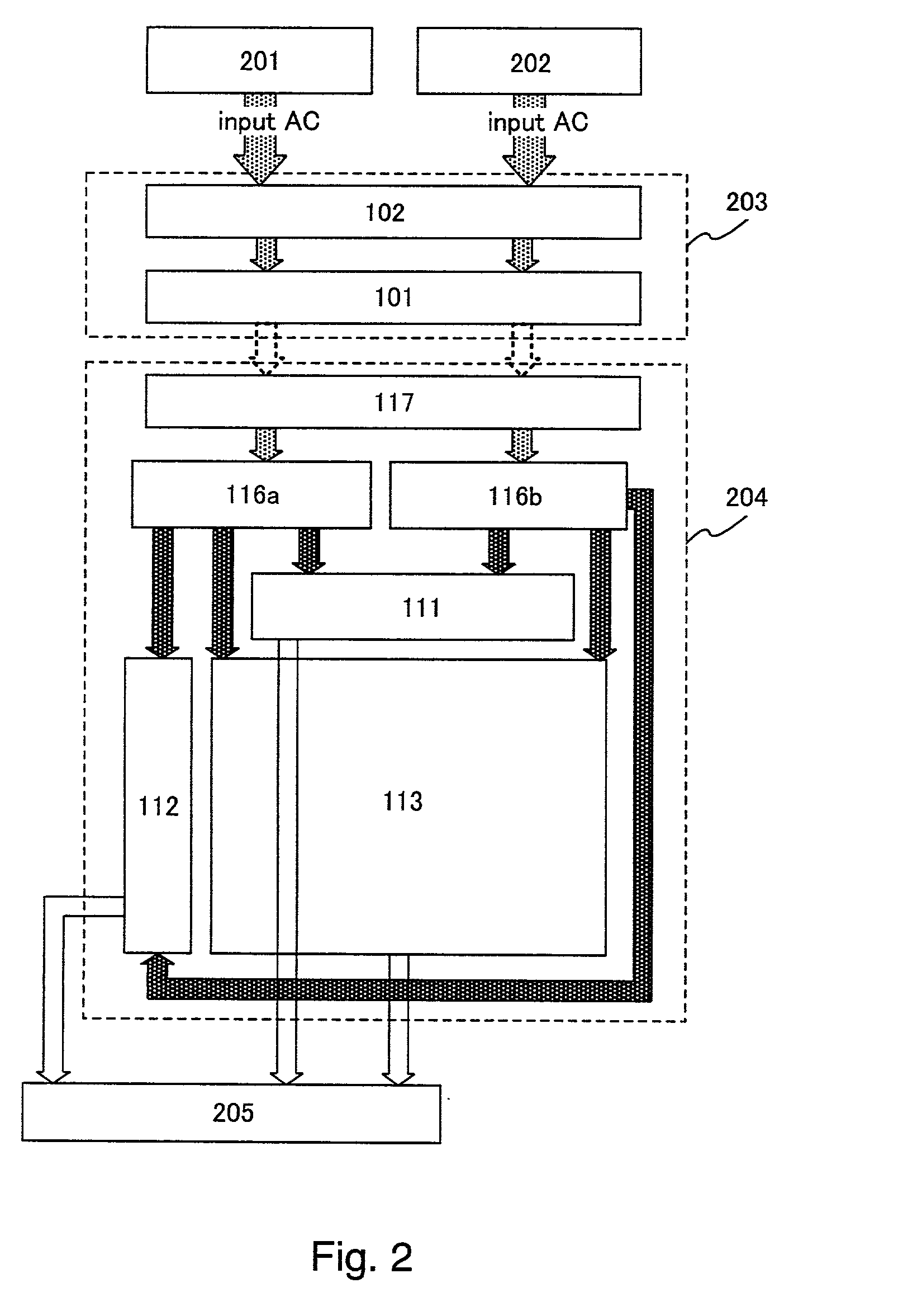
[0018] Then, the primary coils of the inspection substrate and the secondary coils of the device substrate are superimposed on each other so that a certain space is maintained therebetween. Following this, an electromotive force is generated between two terminals of each secondary coil by applying an AC voltage between two terminals of each primary coil. Note that it is preferable that this space is reduced as much as possible and a primary coil forming unit and a secondary coil forming unit are positioned so that a space between them is reduced as much as possible to the extent that the space can be controlled.
[0024] With the present invention, there is realized the structures described above. Therefore, it becomes possible to detect each defective spot without directly setting up probes on wires. As a result, there is prevented the reduction of yield in the following steps due to minute dust caused by the setting up of probes. In addition, unlike the optical inspection method, it becomes possible to judge whether all of pattern forming steps have been successfully done by a single inspection step. As a result, the inspection step is further simplified.

Problems solved by technology

In the case of the optical inspection method, if an inspection is performed after the formation of several pattern layers is finished, it becomes difficult to identify patterns formed as lower layers and therefore it is difficult to detect each defective spot.
However, if an inspection is performed each time a pattern is formed, the inspection step itself becomes complicated and the time taken by the whole manufacturing steps is elongated.
Also, in the case of the probe inspection method, probes are directly set up on wires, so that there may be cases where the wires are damaged and minute dust is caused.
As a result, there is prevented the reduction of yield in the following steps due to minute dust caused by the setting up of probes.
However, if a large-capacity capacitor is formed to make it possible to sufficiently flatten the pulsating current using a thin-film semiconductor, the area of the capacitor itself becomes extremely large.
Therefore, this method is unrealistic.

Method used


Image

  • Inspection method and inspection apparatus
  • Inspection method and inspection apparatus
  • Inspection method and inspection apparatus

Examples


first embodiment

[0097] In this embodiment, there will be described an example in which an electric field generated in each circuit or circuit element is detected using an electrooptic effect in an inspection step. In more detail, in this embodiment, there will be described an example in which measurements are performed using a Pockels cell.

[0098] The Pockels cell is one type of an electrooptic element that uses the Pockels effect that is one electrooptic effect. Note that the electrooptic element is an element that uses an electrooptic effect with which a refractive index is changed by the application of an electric field. By utilizing this property, it becomes possible to use the electrooptic element as a shutter, and to use it to modulate light, and to generate or detect circular polarization by applying an AC voltage or a pulse voltage to a crystal.

[0099] FIG. 9A shows a state where a device substrate 901 of a liquid crystal display and a Pockels cell 909 are superimposed on each other.

[0100] Th...

second embodiment

[0115] In this embodiment, the driving signal and power supply voltage for inspection will be described in more detail by taking, as examples, cases of a liquid crystal display and an OLED display.

[0116] The number of the primary coils and the number of the secondary coils are changed in accordance with the structures of the pixel unit and the driving circuit of the device substrate, so that it is important to set these numbers in accordance with the specifications of each device substrate.

[0117] FIG. 10 shows the structure of a device substrate of a general liquid crystal display. The device substrate shown in FIG. 10 includes a signal line driving circuit 700, a scanning line driving circuit 701, and a pixel unit 702.

[0118] A plurality of signal lines and a plurality of scanning lines are formed in the pixel unit 702 and the areas surrounded by the signal lines and the scanning lines are the equivalent of pixels. Note that in FIG. 10, among a plurality of pixels, only a pixel havi...

third embodiment

[0150] In this embodiment, there will be described a line for cutting a substrate after an inspection is finished.

[0151] FIG. 12 is a top view of a device substrate to be inspected with the inspection method of the present invention. Note that in this embodiment, the inspection method of the present invention will be described by taking, as an example, a device substrate of a liquid crystal display. However, the use of the inspection method of the present invention is not limited to a liquid crystal display but may be used for any other semiconductor devices so long as the semiconductor devices are formed using semiconductors.

[0152] As to the device substrate shown in FIG. 12, a signal line driving circuit 411, scanning line driving circuits 412, a pixel unit 413, leading wires 414, connector connecting units 415, waveform shaping circuits or rectifier circuits 416, secondary coil forming units 417, and coil wires 418 are provided on a substrate 410. Note that in this specification,...


PUM


Abstract

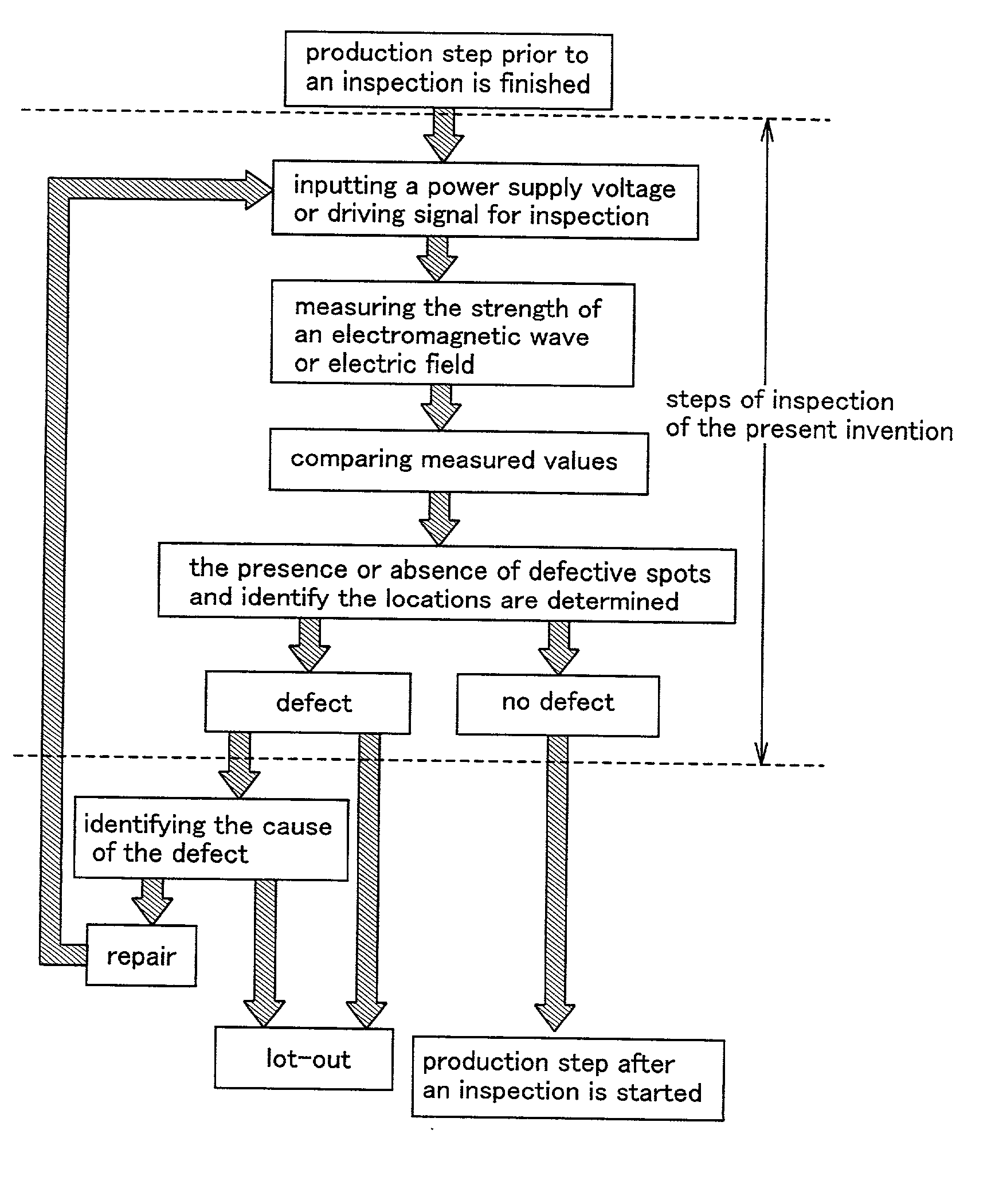
There is established an easier inspection method with which it is not required to set up probes on wires. Also, there is provided an inspection apparatus using this inspection method. With the inspection apparatus or inspection method, primary coils of an inspection substrate and secondary coils of a device substrate are superimposed on each other so that a certain space is maintained therebetween. An AC signal is inputted into the primary coils, thereby generating an electromotive force in each secondary coil by electromagnetic induction. Then, each circuit provided on the device substrate is driven using the electromotive force and information possessed by an electromagnetic wave or electric field generated in this circuit is monitored, thereby detecting each defective spot.

Description

[0001] 1. Field of the Invention[0002] The present invention relates to an inspection apparatus used for a device substrate of a semiconductor device and to an inspection method using the inspection apparatus. More particularly, the present invention relates to an inspection apparatus of non-contact type and an inspection method using the inspection apparatus.[0003] 2. Description of the Related Art[0004] In recent years, attentions have been given to a technique of forming a thin-film transistor (TFT) using a semiconductor film (whose thickness is about several nm to several hundred nm) formed on a substrate having an insulating surface. This is because there is increasing demand for an active matrix semiconductor display device that is one type of semiconductor devices. Typical examples of the active matrix semiconductor display device include a liquid crystal display, an OLED (organic light emitting device) display, and a DMD (digital micromirror device).[0005] It is possible to ...

Claims


Application Information

Patent Timeline
Patent Type & Authority Applications(United States)
IPC IPC(8): G01R31/315G09G3/00
CPCG01R31/3025G01R31/315G09G3/006
Inventor HIROKI, MASAAKI
Owner SEMICON ENERGY LAB CO LTD
Learn More