Semiconductor device and manufacturing method therefor, circuit substrate, and electronic apparatus

a technology of semiconductor devices and semiconductor elements, applied in semiconductor devices, semiconductor/solid-state device details, electrical devices, etc., can solve the problems of unlikely reliability in electrical connection, limit in miniaturization, etc., and achieve the effect of suppressing the strength of semiconductor elements due to penetration hole formation and reducing the energy for forming penetration holes

Inactive Publication Date: 2002-10-17
SAMSUNG ELECTRONICS CO LTD
View PDF7 Cites 122 Cited by
  • Summary
  • Abstract
  • Description
  • Claims
  • Application Information

AI Technical Summary

Benefits of technology

0024] (3) In this manufacturing method for the semiconductor device, the intermediate portion may be formed such that all parts have nearly the same diameter, and the penetration hole may be formed in the shape further including a taper portion connecting the open end portion and the intermediate portion. According to this, since all parts of the intermediate portion have nearly the same diameter, stress is applied evenly and, therefore, reduction of strength of the semiconductor element due to formation of the penetration hole can be suppressed.
0025] (4) In this manufacturing method for the semiconductor device, in the first step, a small hole having a diameter smaller than that of the penetration hole may be formed in advance, and the small hole may be enlarged so as to form the penetration hole. According to this, the small hole can be formed with energy smaller than that in the formation of the penetration hole and, therefore, the energy for forming the penetration hole can be reduced by forming the small hole in advance.

Problems solved by technology

However, since the wire, etc., have been provided, there has been a limitation in miniaturization.
However, when a narrow penetration hole is filled with solder, a void is generated and, therefore, reliability in electrical connection is unlikely to be ensured.

Method used


Image

  • Semiconductor device and manufacturing method therefor, circuit substrate, and electronic apparatus
  • Semiconductor device and manufacturing method therefor, circuit substrate, and electronic apparatus
  • Semiconductor device and manufacturing method therefor, circuit substrate, and electronic apparatus

Examples


Embodiment Construction

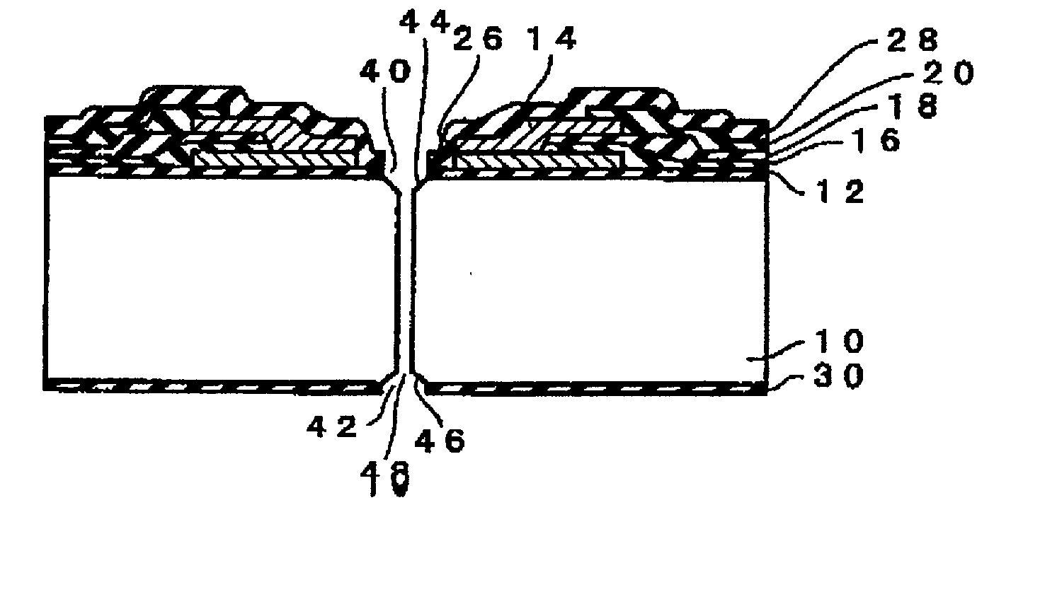
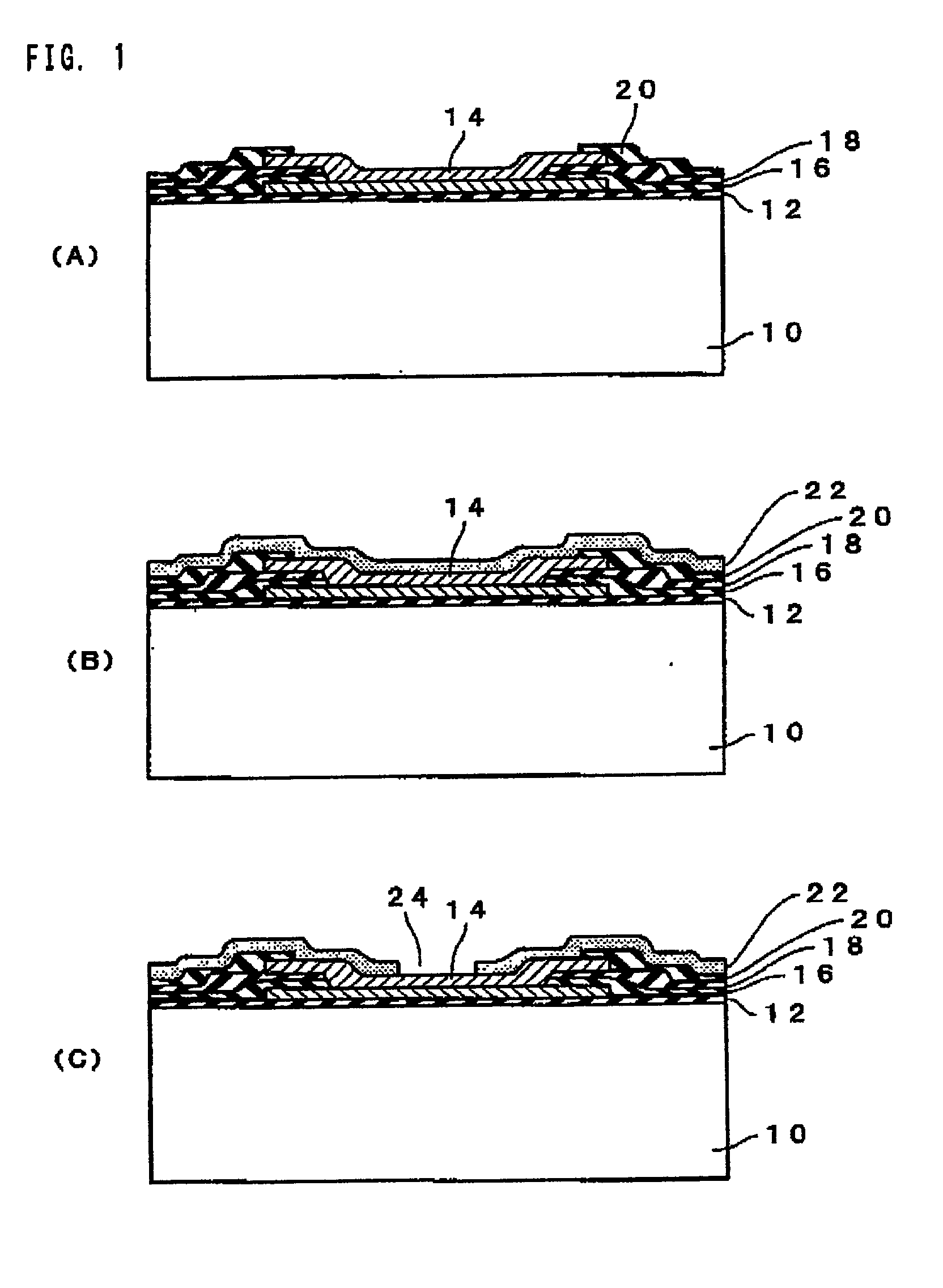
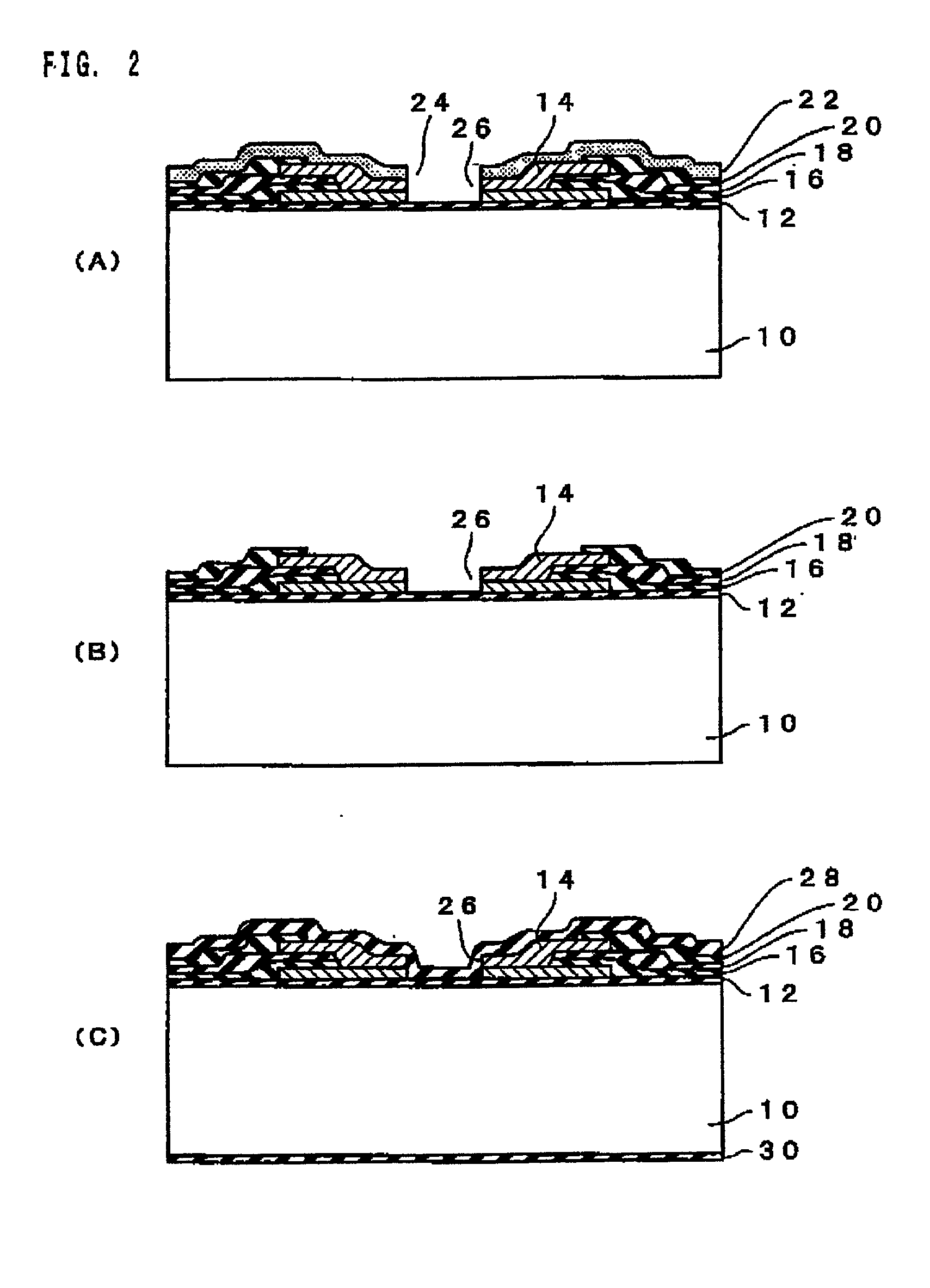
[0045] Preferred embodiments according to the present invention will be described below with reference to the drawings. FIG. 1(A) is a diagram showing a part of a semiconductor chip 10 used in the present embodiment. In general, the semiconductor chip 10 is a rectangular parallelepiped (including a cube). However, the shape thereof is not limited, and may be the shape of a sphere.

[0046] The semiconductor chip 10 includes an insulating film (interlayer film) 12 on the surface on which an integrated circuit, although not shown in the drawing, composed of transistors, memory elements, etc., is formed. In many cases, the insulating film 12 is an oxide film of silicon which is a basic material for the semiconductor chip 10. An electrode (pad) 14 is formed on the insulating film 12, and the electrode 14 is electrically connected to the integrated circuit at the part not shown in the drawing. In many cases, the electrode 14 is formed from aluminum. The electrode 14 is aligned along at leas...


PUM


Abstract

A semiconductor device and a manufacturing method therefor, a circuit substrate, and electronic apparatus are provided, in which electrical connection can be performed with high reliability and with ease. The manufacturing method for a semiconductor device includes the steps of forming a penetration hole 50 in a semiconductor chip 10 having an electrode 14, and forming a conductive layer 70 in the region including the inside of the penetration hole 50. Regarding the penetration hole 50, an intermediate portion is formed to be larger than an open end portion, and the conductive layer 70 is formed by applying a coating of a liquid containing metal fine particles by an ink-jet method.

Description

[0001] The present invention relates to a semiconductor device and a manufacturing method therefor, a circuit substrate, and electronic apparatus.[0002] In recent years, semiconductor devices have been developed, in which a plurality of semiconductor chips are laminated. The majority thereof have been those in which bonding of a wire or a lead to an electrode of the semiconductor chip is performed for the sake of electrical connection. However, since the wire, etc., have been provided, there has been a limitation in miniaturization. It has also been developed to perform electrical connection by forming a penetration hole in a semiconductor chip and filling the penetration hole with molten solder. However, when a narrow penetration hole is filled with solder, a void is generated and, therefore, reliability in electrical connection is unlikely to be ensured.[0003] The present invention is to overcome this problem. It is an object of the present invention to provide a semiconductor dev...

Claims


Application Information

Patent Timeline
Patent Type & Authority Applications(United States)
IPC IPC(8): H01L21/288H01L21/3205H01L21/768H01L23/52H01L25/065H01L25/07H01L25/18H01L29/41
CPCH01L21/288H01L2224/16145H01L21/76898H01L24/03H01L24/05H01L2224/05001H01L2224/05022H01L2224/05572H01L2924/00014H01L2224/05599H01L2224/05124
Inventor FURUSAWA, MASAHIRO
Owner SAMSUNG ELECTRONICS CO LTD
Why Eureka
Try Eureka