Module with built-in electronic elements and method of manufacture thereof

a technology of electronic elements and modules, which is applied in the direction of electrical apparatus construction details, generators/motors, printed circuit non-printed electric components association, etc., can solve the problems of difficult to achieve high-density packaging, the inner structure of high-density mounted circuit boards having such a via hole cannot keep up with the miniaturization of semiconductor chips, and become an obstacle to the miniaturization of semiconductor packages, etc., to achieve the effect of manufacturing such an electric element built-in modules

Inactive Publication Date: 2002-10-31
PANASONIC CORP
View PDF0 Cites 116 Cited by
  • Summary
  • Abstract
  • Description
  • Claims
  • Application Information

AI Technical Summary

Benefits of technology

0024] It is an object of the present invention to solve the conventional problems described above and to provide a thin and mechanically strong module containing electric elements such as s

Problems solved by technology

However, with conventional multilayered circuit boards including glass fiber and an epoxy resin (glass-epoxy multilayered circuit boards) having a penetrating through hole structure formed by drilling, it has become difficult to achieve the high-density packaging.
However, with the current state of the art, even the high-density mounted circuit boards having such an inner via hole structure cannot keep up with the miniaturization of the semiconductor chips.
Therefore, the space for leading out the electrodes from the semiconductor chips increases, thus becoming an obstacle to miniaturization of the semiconductor packages.
Also, since the circuit boards are formed with a resin-based material, they have a low thermal conductivity.
Thus, as the component packaging achieves a higher density, it becomes more difficult to dissipate heat that is generated from these components.
Furthermore, along with the increase in speed and density, it has become difficult to ignore the influence of noise.
In any methods, it is needless to say that the semiconductor chip should be as thin as possible, but since the one (a silicon semiconductor, in particular) with a thickness of not more than 100 .mu.m has a poor mechanical strength, such a semiconductor chip sometimes is damaged during the flip-chip mounting, in which a load is a

Method used


Image

  • Module with built-in electronic elements and method of manufacture thereof
  • Module with built-in electronic elements and method of manufacture thereof
  • Module with built-in electronic elements and method of manufacture thereof

Examples


first example

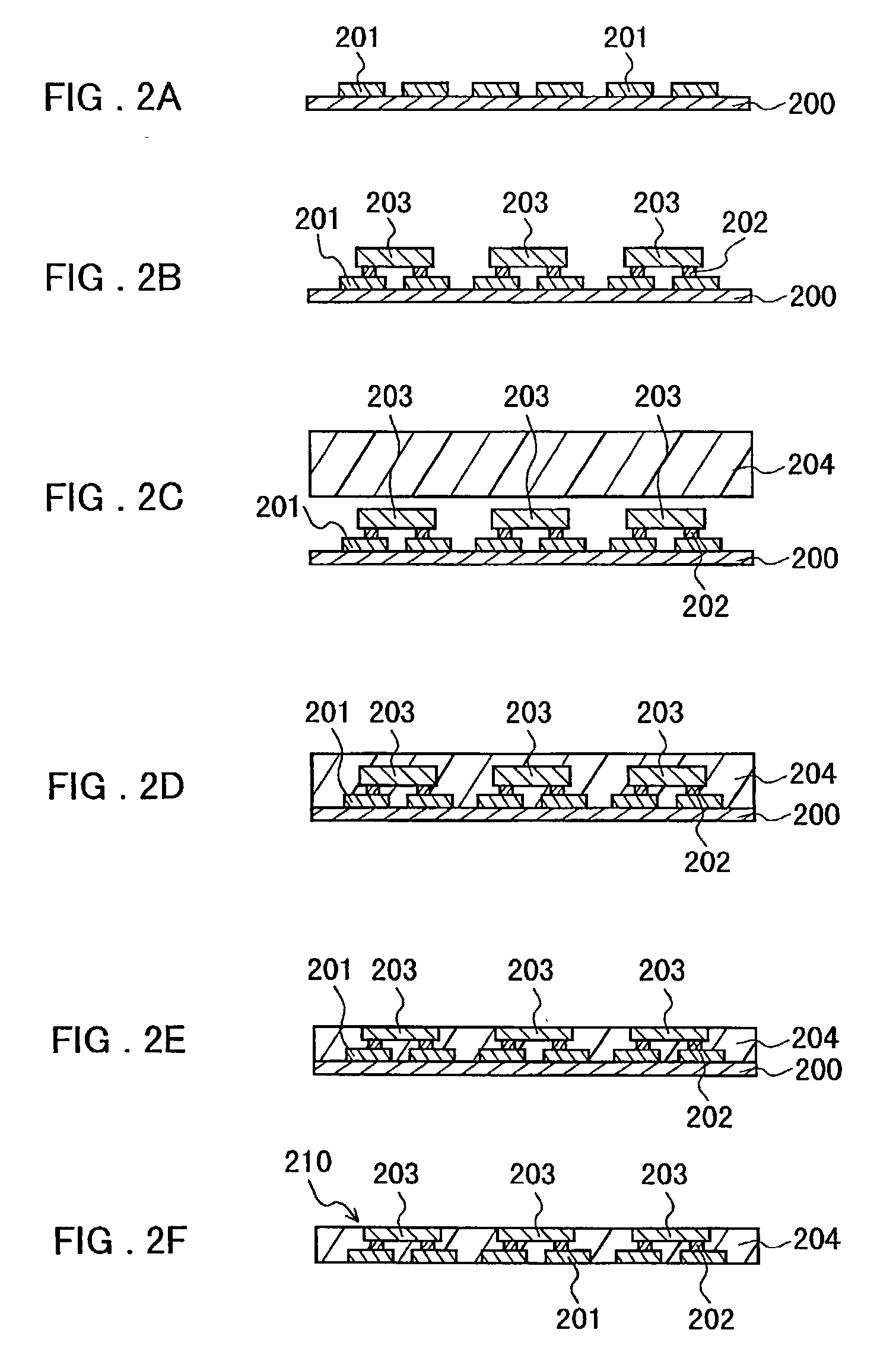
[0142] The following is a description of an example corresponding to the first embodiment described above.

[0143] First, the method for producing the copper-foil support 200, shown in FIG. 2A, whose surface is provided with the wiring patterns 201 will be explained.

[0144] An existing copper foil for a circuit board can be used for the copper-foil support 200. Such a copper foil was produced by rotating a drum electrode in an electrolyte and continuously reeling in a copper plating layer formed on this drum. At this time, by adjusting the current value and the rotation speed for forming the plating layer, it was possible to form a copper foil with a desired thickness continuously. The thickness of the copper foil used here was 70 .mu.m.

[0145] Next, a peel-off layer for a later transferring was formed by forming an extremely thin organic layer on the surface of this copper-foil support 200 or by plating metal that is different from the copper, such as nickel or tin, thinly thereon. The...

second example

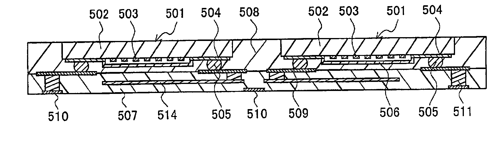
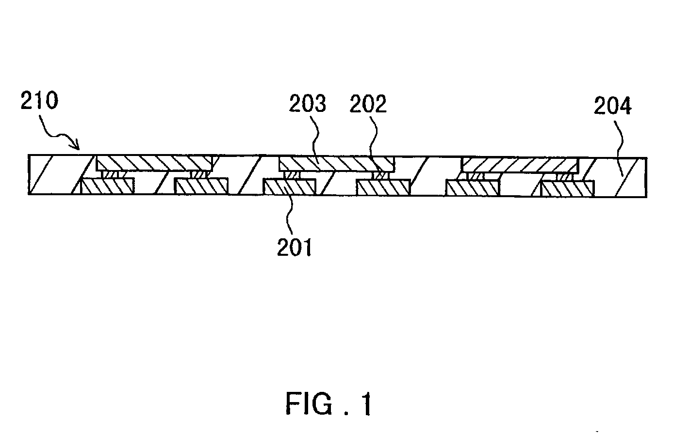
[0180] The following is a description of an example corresponding to the second embodiment described above. Illustrated is an example of manufacturing a semiconductor chip built-in module having a multilayered structure using an abraded semiconductor chip built-in module 210 that has been produced by a method similar to the first example.

[0181] As shown in FIG. 4A, the semiconductor chip built-in module 210 that had been produced in the first example, the prepreg 401 for the circuit board and the copper foil 405 were multilayered.

[0182] The prepreg 401 for the circuit board was obtained by impregnating a glass fabric with an epoxy resin so as to be in the B stage. The thickness thereof was 100 .mu.m. This prepreg was cut into a predetermined size, and then through holes having a diameter of 0.15 mm were formed at a constant pitch of 0.2 to 2 mm using a carbon dioxide gas laser.

[0183] Using a three roll mill, 85 wt % of spherical copper particles, 3 wt % of bisphenol A type epoxy res...


PUM

PropertyMeasurementUnit
Timeaaaaaaaaaa
Temperatureaaaaaaaaaa
Timeaaaaaaaaaa

Abstract

At least two electric elements (203) such as semiconductor chips or surface acoustic wave devices are mounted on wiring patterns (201), and the electric elements (203) are sealed with a thermosetting resin composition (204). An upper surface of the at least two electric elements (203) and an upper surface of the thermosetting resin composition (204) are abraded at the same time, thereby forming surfaces substantially flush with each other. Since they are abraded while being sealed with the thermosetting resin composition (204), it is possible to reduce the thickness without damaging the electric elements (203). Also, the electric elements (203) and the wiring patterns (201) can be prevented from being contaminated by an abrasive liquid. In this manner, it is possible to obtain an electric element built-in module whose thickness can be reduced while maintaining its mechanical strength.

Description

[0001] The present invention relates to a module containing electric elements such as semiconductor chips or surface acoustic wave devices. In particular, the present invention relates to an electric element built-in module that can be made ultra-thin and is suitable for a high-density packaging. In addition, the present invention relates to a method for manufacturing such an electric element built-in module.[0002] In recent years, with the demand for higher performance and miniaturization of electronic equipment, higher density and higher function for packages in which semiconductor chips are mounted have been desired increasingly. Furthermore, there also is an increasing demand for smaller and higher-density circuit boards on which they are mounted. However, with conventional multilayered circuit boards including glass fiber and an epoxy resin (glass-epoxy multilayered circuit boards) having a penetrating through hole structure formed by drilling, it has become difficult to achiev...

Claims


Application Information

Patent Timeline
IPC IPC(8): H01L21/56H01L21/68H01L23/31H05K1/18
CPCH01L21/561Y10T29/53178H01L23/3107H01L24/96H01L24/97H01L2224/97H01L2924/01003H01L2924/01013H01L2924/01015H01L2924/01027H01L2924/01029H01L2924/0103H01L2924/01032H01L2924/01033H01L2924/01039H01L2924/01047H01L2924/01074H01L2924/01078H01L2924/01079H01L2924/01082H01L2924/10329H01L2924/16195H01L2924/18161H01L2924/19041H01L2924/19042H01L2924/19043H05K1/187H05K3/20H05K3/4069H05K3/4614H05K3/4652H05K2201/10378H01L21/568Y10T29/49135H01L2224/16225H01L2224/16245H01L2924/01005H01L2924/01006H01L2924/01019H01L2924/12041Y10T29/49146Y10T29/4913Y10T29/53174H01L2224/81H01L2924/15787H01L2924/12042H01L2924/181H01L2224/45144H01L2224/05573H01L2224/05568H01L2924/16235H01L2224/81005H01L2924/00H01L2924/00012H01L2224/05624H01L2924/00014H01L23/50
Inventor NAKATANI, SEIICHIBESSHO, YOSHIHIROSUGAYA, YASUHIROONISHI, KEIJI
Owner PANASONIC CORP
Why Eureka
Try Eureka