Method and apparatus for producing VCSELS with dielectric mirrors and self-aligned gain guide

a technology of dielectric mirrors and gain guides, which is applied in electrical apparatus, semiconductor lasers, laser details, etc., can solve the problems of thermal expansion coefficient, material strain, and complicating fabrication processes and device operation, so as to reduce the resistance in the top dbr, reduce the straggle of implants, and limit the photolithography steps

Inactive Publication Date: 2002-12-19
II VI DELAWARE INC
View PDF2 Cites 13 Cited by
  • Summary
  • Abstract
  • Description
  • Claims
  • Application Information

AI Technical Summary

Benefits of technology

0011] The invention provides a small diameter, low threshold current VCSEL with reduced resistance in the top DBR. At least 90% of the top semiconductor DBR is replaced by a dielectric mirror fabricated over only the output aperture of the VCSEL. Device current has only to pass through a few layers of the high resistance semiconductor DBR. The real extent of the dielectric mirror is never larger than the laser aperture throughout fabrication. As a result, a minimum amount of stress is exerted on the device.
0012] At the same time, the invention provides an aligned gain guide while at the same time limiting photolithography steps. Implant straggle is also reduced as most of the top semiconductor DBR material has been eliminated. As a result, a lower energy implant can be used, allowing for the previously deposited dielectric mirror to function as a self-aligned implant mask. The result is potentially a smaller current confining aperture.

Problems solved by technology

This approach raises concern because of the difference in coefficients of thermal expansion between the dielectric thin film and the other materials used in the VCSEL.
The difference in coefficients of thermal expansion causes strains between the materials and can complicate fabrication processes and device operation.
Small diameter apertures are often difficult to fabricate with ion implantation techniques because of proton straggle.
However, Mori et al. do not address the problems of VCSELs beyond those solutions discussed above.

Method used


Image

  • Method and apparatus for producing VCSELS with dielectric mirrors and self-aligned gain guide
  • Method and apparatus for producing VCSELS with dielectric mirrors and self-aligned gain guide
  • Method and apparatus for producing VCSELS with dielectric mirrors and self-aligned gain guide

Examples


Embodiment Construction

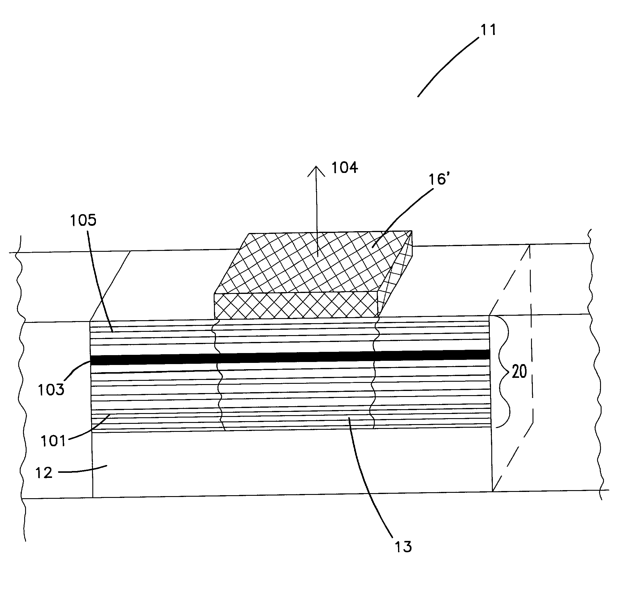
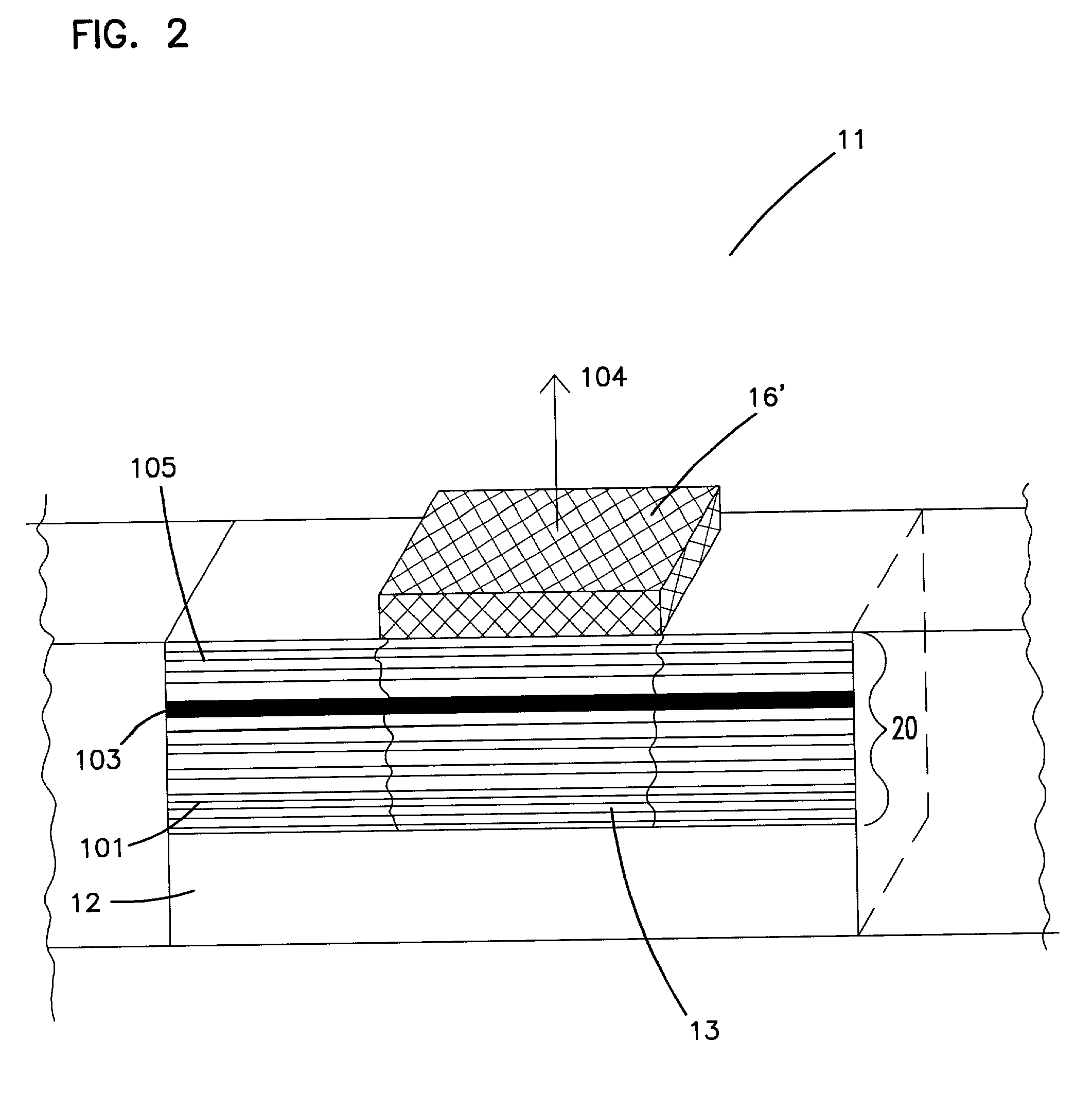
[0020] While FIGS. 1 through 10 represent single devices, it should be understood that numerous devices can be fabricated on a substrate, for example, in an array arrangement. Additionally, it should be understood that FIGS. 1 through 10 are sectional views, therefore illustrations depicted in FIGS. 1 through 10 can extend into and out of the drawings.

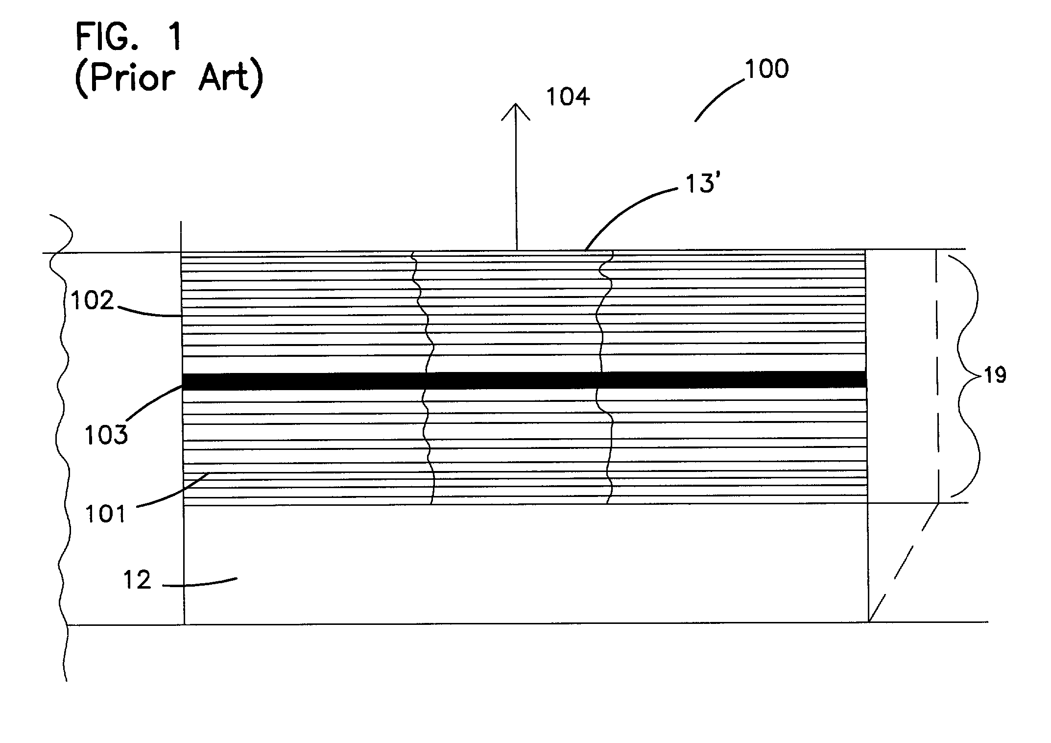
[0021] FIG. 1 depicts a VCSEL 100 of the prior art. As shown in FIG. 1, the VCSEL 100 includes a number of elements: substrate 12, and epitaxial layers 19, which comprises a bottom stack of semiconductor distributed Bragg reflectors (DBR) 101, a top semiconductor DBR stack 102, and an active region 103. Light output 104 is perpendicular to the substrate 12 and is emitted from VCSEL 100 from the laser area 13'.

[0022] VCSEL 100 is fabricated by growing epitaxial layers 19 on the substrate 12. First, bottom semiconductor DBR stack 101 is grown. For example, bottom semiconductor DBR stack 101 can be made of pairs of alternating layers of a...


PUM


Abstract

The invention includes a method of fabricating a laser device, that includes: depositing a photoresist on epitaxially grown layers, patterning said photoresist to form an aperture area, depositing a dielectric material on said patterned photoresist, depositing a liftoff layer on said dielectric material, removing portions of said dielectric material and liftoff layer that border said aperture area, implanting regions of the epitaxially grown layers bordering said aperture area, and depositing a metal layer on said dielectric material. The invention also includes a device including: a substrate comprising epitaxial layers and an aperture area, a dielectric mirror formed on top of said aperture area and an implanted region within said epitaxial layers, said implanted region bordering said aperture area.

Description

[0001] The invention relates generally to vertical cavity surface emitting lasers (VCSELs) and methods for producing these lasers. More specifically, the invention relates to methods for the fabrication of low resistance, small diameter, low threshold current laser devices.[0002] Reducing electrical resistance and threshold current is of primary importance in producing highly efficient and reliable vertical cavity surface emitting laser (VCSEL) devices.[0003] The electrical resistance of a VCSEL can be lowered by reducing the resistance of the materials used to fabricate the VCSEL. The physical structure of the VCSEL can also be optimized to reduce resistance by altering the width and length of the conduction path.[0004] A large portion of the overall electrical resistance of the VCSEL may be attributed to the semiconductor distributed Bragg reflectors (DBR) used as the input and output mirrors of the laser cavity. One means of reducing resistance of the DBR components is to replace...

Claims


Application Information

Patent Timeline
Patent Type & Authority Applications(United States)
IPC IPC(8): H01S5/183H01S5/20
CPCH01S5/18308H01S5/2063H01S5/18377H01S5/18369H01S5/183
Inventor SKOGMAN, RICHARD A.
Owner II VI DELAWARE INC
Why Eureka
Try Eureka