Test and debug processor and method

Inactive Publication Date: 2003-03-27
MICHAEL SAM
View PDF21 Cites 21 Cited by
  • Summary
  • Abstract
  • Description
  • Claims
  • Application Information

AI Technical Summary

Benefits of technology

0023] Any of these features if integrated in the current solution will help increase the test speed

Problems solved by technology

With the complexity and increase of pin-count of new computer chips and the dense assembly of these chips on circuit boards, it becomes increasingly difficult to test and debug the circuit boards after being assembled.
It should be understood that a substantial amount of time is wasted due to the relatively extensive communications between the test-tool CPU, the memory and the test-bus controller.
One of the major difficulties of adding an instruction FIFO is the need to synchronize the instruction FIFO with the data FIFO.
Secondly, because the test-bus controller cannot execute any logic operations, it has to wait for the main CPU to execute these operations to test the incoming data from the test board.
With the

Method used


Image

  • Test and debug processor and method
  • Test and debug processor and method
  • Test and debug processor and method

Examples


Embodiment Construction

)

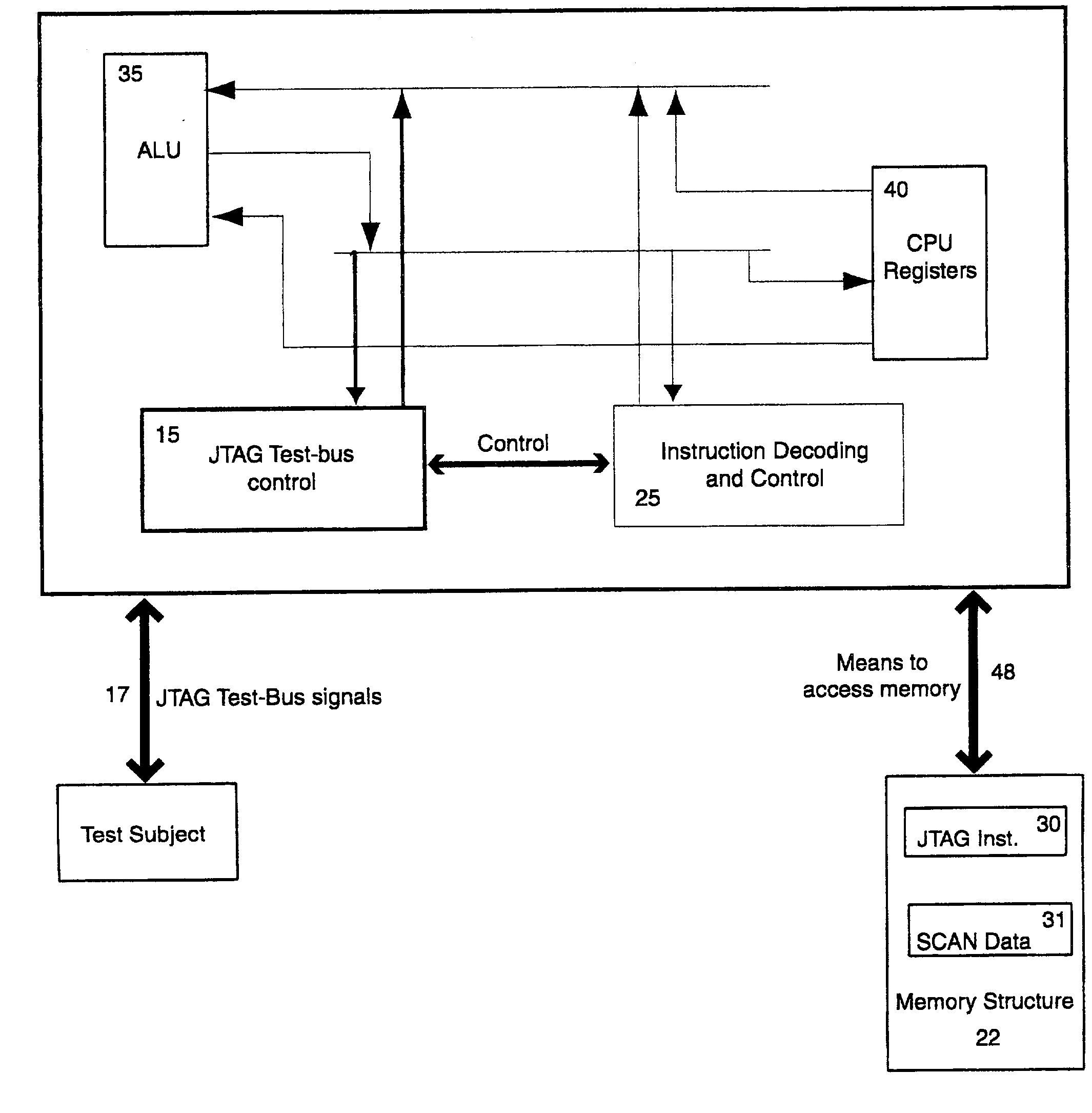
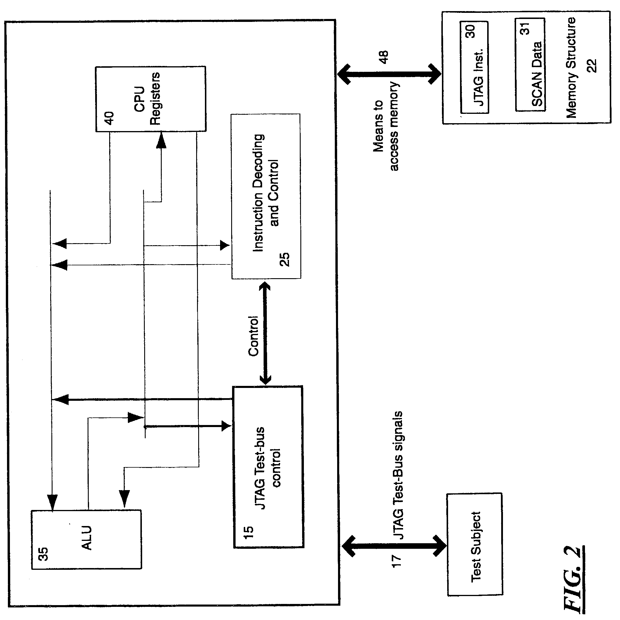
[0026] Referring to the accompanying FIG. 2, there is shown and described a test and debug processor 10 that can execute native test instructions. The processor 10 includes a JTAG-bus controller 15 with a JTAG port 17 coupled thereto, a memory means 20 or 22 capable of storing JTAG instructions 30 and scan data 31, and an instruction encoding unit 25 capable of fetching or requesting JTAG instructions from the memory means 20 or 22. The processor 10 may also include an optional ALU 35 and a memory-bus controller 48 connected to the JTAG-bus controller logic 15 making it a bus master. For example, in the case of a JTAG, the CPU can execute a SCAN_IR or SCAN_DR instruction directly after fetching it from memory. An example for such an instruction would be SIR R5, R6. This will let the CPU choose the SCAN_IR JTAG state and send all or part of the contents of register 5 (R5) to the test board. The data coming back from the test board will be stored in register 6 (R6). Another example w...


PUM


Abstract

A Test and debug processor that can execute JTAG scans without the involvement of an external CPU or dedicated hardware. The processor includes a JTAG-bus controller logic, a JTAG port coupled to the JTAG-bus controller logic, memory capable of storing JTAG instructions, and an instruction decoding unit capable of fetching or requesting JTAG instructions from the memory. During use, the JTAG scan functions are encoded in instructions that are natively executable by the processor hardware without software interpretation. The instructions are then stored in a memory structure, fetched and executed directly by the processor. The instruction could optionally include the end-state of the bus after the operation, information about the bit count of the data to be scanned, information about the location of the data to be sent out of the JTAG port and also the location to store the received information from the test subject. Optionally, the test processor can directly access any memory location to fetch or store test data objects. This is achieved by adding a memory-bus interface to the processor allowing it to be the memory bus master. Also the test-processor can have the ability to decode and execute arithmetic and logic operation by adding an ALU the processor. The processor can also have the ability to execute register transfer operations to execute functions such as JUMP to control the run path.

Description

[0001] This application claims the benefit of U.S. Pat. No. 60 / 324,240 filed on Sep. 21, 12, 2001.[0002] 1. Field of the Invention[0003] This invention pertains to electronic devices used to test and debug electrical circuits, more particularly, such devices that use a Joint Test Action Group (JTAG) port.[0004] 2. Description of the Related Art[0005] With the complexity and increase of pin-count of new computer chips and the dense assembly of these chips on circuit boards, it becomes increasingly difficult to test and debug the circuit boards after being assembled. A group of leading electronic companies has joint forces and developed a standard test port to be built on every chip. The purpose of this test port is to allow connection to a test tool to check the value of each pin on the chip. Some chips add more functionality to this test port to provide access to virtually any resource inside the chip. One example of an in situ test port is the so called "JTAG" (Joint Test Action Gr...

Claims


Application Information

Patent Timeline
IPC IPC(8): G06F11/36
CPCG06F11/2236
Inventor MICHAEL, SAM
Owner MICHAEL SAM
Why Eureka
Try Eureka