Liner with poor step coverage to improve contact resistance in W contacts
a technology of w contacts and step coverage, applied in the direction of basic electric elements, electrical apparatus, semiconductor devices, etc., can solve the problem of widening the resistance spread
- Summary
- Abstract
- Description
- Claims
- Application Information
AI Technical Summary
Benefits of technology
Problems solved by technology
Method used
Image
Examples
Embodiment Construction
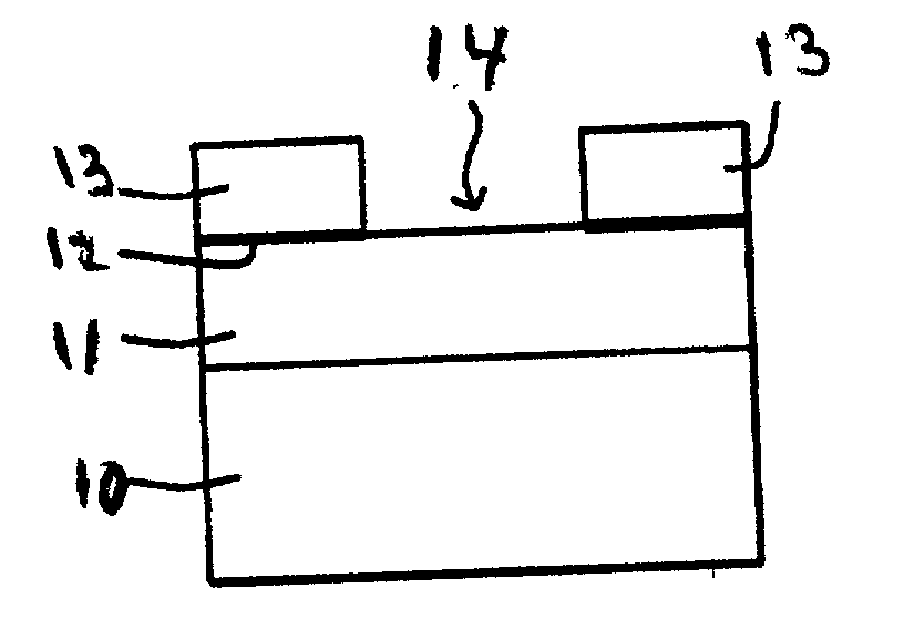
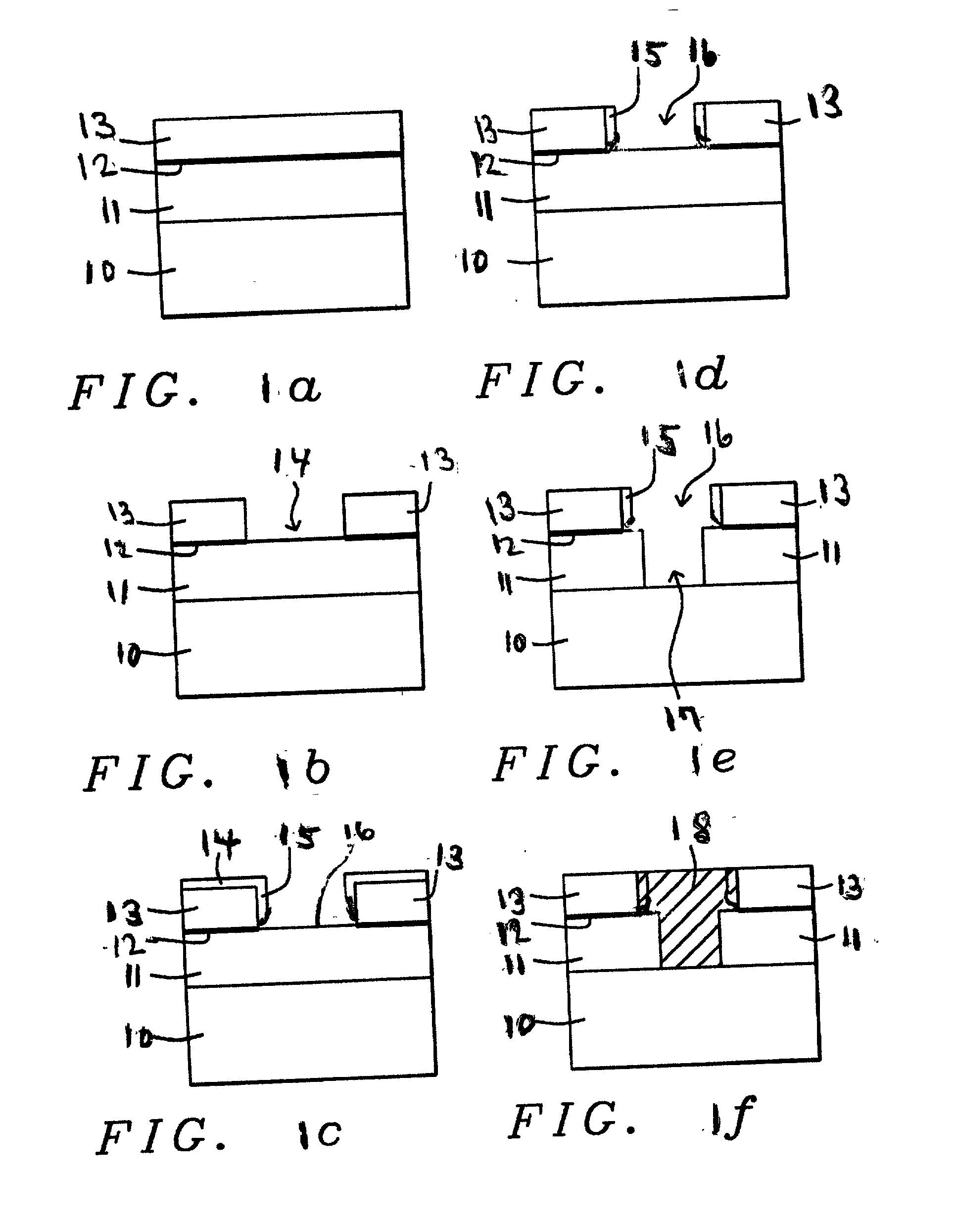
[0027] The present invention is directed to fabricating and manufacturing a current carrying metal filled contact / vias of sub-micron diameter using a liner with poor step coverage to improve the contact resistance in W contacts. The process can be used in MOSFET or CMOS or any high density semiconductor device presently being manufactured in the semiconductor industry; however, only those specific areas unique to comprehension of this invention will be described.
[0028] In general, a conductive plug filling a via hole is formed by depositing an interlayer dielectric (ILD) on a conductive layer comprising at least one conductive layer comprising at least one conductive pattern, forming an opening through the ILD by photolithographic and etching techniques, and filling the opening with a conductive material. Excess conductive material on the surface of the ILD is generally removed by chemical mechanical polishing (CMP). One such method is known as the single damascene technique and ent...
PUM
 Abstract
Description
Claims
Application Information

