Method for forming capacitor of a semiconductor device

a technology of semiconductor devices and capacitors, applied in solid-state devices, coatings, chemical vapor deposition coatings, etc., can solve the problems of reducing the electrical characteristics of capacitors of semiconductor devices, difficult to obtain sufficient capacitance, and reducing the electrical characteristics of capacitors, so as to achieve the height of capacitors and capacitors sufficient for highly integrated semiconductor devices

Inactive Publication Date: 2003-06-12
SK HYNIX INC
View PDF0 Cites 17 Cited by
  • Summary
  • Abstract
  • Description
  • Claims
  • Application Information

AI Technical Summary

Benefits of technology

[0020] Accordingly, a method for forming a capacitor of a semiconductor device is disclosed wherein oxygen in the Ru film is removed to prevent degradation of characteristics of devices generated during the subsequent thermal treatment process and of Ru film having rugged surface to obtain a sufficiently high capacitance.
[0042] The oxygen in the Ru film is removed by injecting NH.sub.3 gas during the deposition process of the Ru film which is used as electrode for deoxidation. Further, formation of an oxide film at the interface of Ru film and barrier metal layer is prevented by performing NH.sub.3 plasma treatment after the deposition of Ru film to remove oxygen in Ru film. As a result, a capacitance sufficient for highly integrated semiconductor devices is obtained by performing RTP on Ru film under N.sub.2 or NH.sub.3 gas atmosphere to form a rugged surface without increasing the height of capacitor.

Problems solved by technology

As the cell size is decreased due to high integration of semiconductor devices, it is difficult to obtain sufficient capacitance which is proportional to the surface area of storage electrode.
However, during the subsequent thermal treatment, oxygen atoms contained in the Ru film, which is the storage electrode oxidize the TiN film in the contact plug and result in the formation of an oxide film.
That is, an oxide film is formed at the interface of the Ru film and the TiN film, which results in degradation of electrical characteristics of capacitors of semiconductor devices and lift-off of Ru films.
In addition, an overhang occurs due to the height requirement of the capacitor in order to provide sufficient capacitance for high integration of semiconductor, which causes degradation of step coverage during the deposition process of Ru film, thereby degrading reliability and characteristics of devices and hinders high integration of semiconductor devices.

Method used


Image

  • Method for forming capacitor of a semiconductor device
  • Method for forming capacitor of a semiconductor device
  • Method for forming capacitor of a semiconductor device

Examples


Embodiment Construction

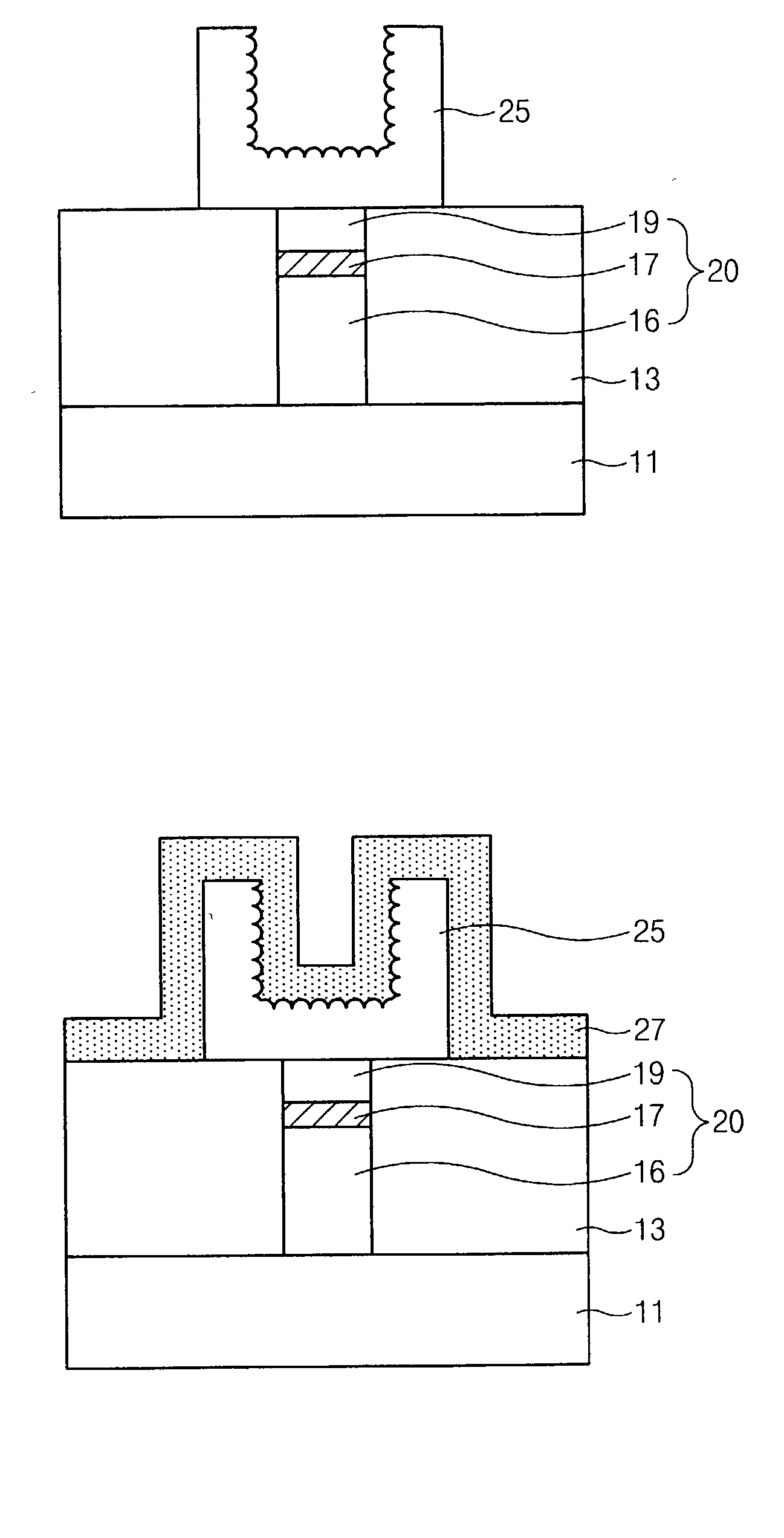
[0045] A method for forming a capacitor of a semiconductor device according to this disclosure will be described in greater detail referring to the accompanying drawings.

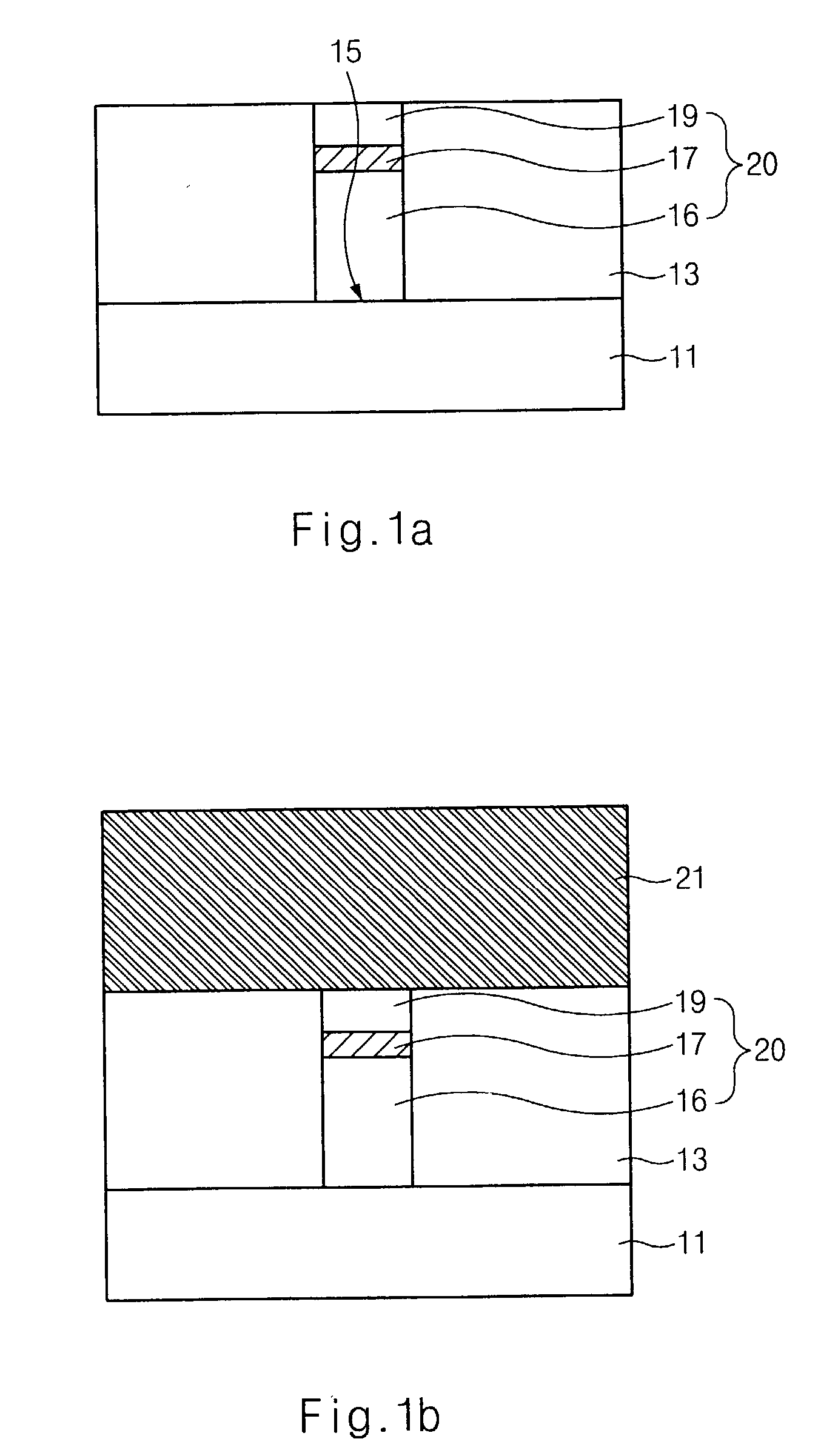
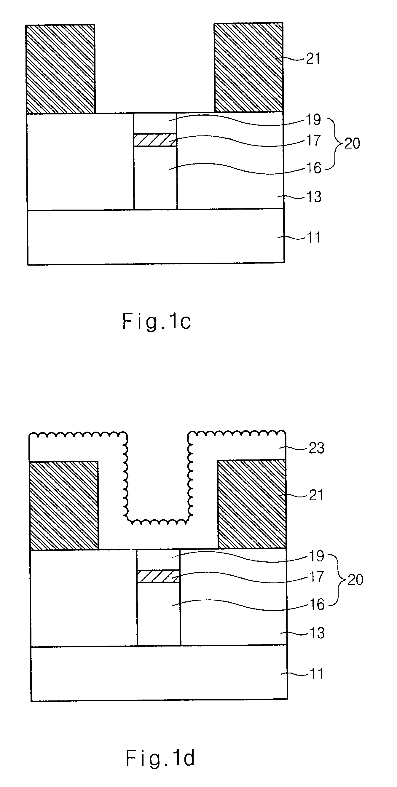
[0046] FIGS. 1a to 1g are cross-sectional diagrams illustrating a method for forming a capacitor of a semiconductor device in accordance with a preferred embodiment, wherein the capacitor is a cylinder type capacitor.

[0047] Referring to FIG. 1a, a planarized lower insulating layer 13 is formed on a semiconductor substrate 11 which comprises a device isolation film (not shown), a word line (not shown) and a bit line (not shown).

[0048] The lower insulating layer 13 is formed of insulating materials having high fluidity such as BPSG.

[0049] Thereafter, a storage electrode contact hole 15 exposing a predetermined portion of the substrate 11 is formed in the lower insulating layer 13.

[0050] The storage electrode contact hole 15 is formed by etching the lower insulating layer 13 via a photo-etching process using a storage ...


PUM

PropertyMeasurementUnit
pressureaaaaaaaaaa
temperatureaaaaaaaaaa
thicknessaaaaaaaaaa

Abstract

A method for forming a capacitor of a semiconductor device which provides improved reliability and characteristics of semiconductor device by removing oxygen from the Ru film using NH3 gas during the deposition process of the Ru film used as storage electrode material or, in the alternative, performing a NH3 plasma treatment after the deposition process of Ru film to inhibit formation of oxide film at the interface of Ru film and barrier metal layer, and then by forming rugged surface on the Ru film with RTP under N2 or NH3 gas atmosphere to obtain a high capacitance for high integration of semiconductor device.

Description

[0001] 1. Technical Field[0002] Methods for forming capacitors of semiconductor devices are disclosed, and more particularly, methods for forming capacitors comprising a dielectric film formed of high dielectric constant material and a storage electrode formed of ruthenium (hereinafter, referred to as "Ru") film are disclosed wherein oxygen in the Ru film is removed to prevent degradation of the electrical characteristics of the devices generated during the subsequent thermal treatment process and further to provide Ru films with rugged surfaces thereby increasing the surface area thereof and obtaining high capacitances of the capacitors.[0003] 2. Description of the Related Art[0004] As the cell size is decreased due to high integration of semiconductor devices, it is difficult to obtain sufficient capacitance which is proportional to the surface area of storage electrode.[0005] Specifically, in case of DRAM device having a unit cell consisting of a MOS transistor and a capacitor, t...

Claims


Application Information

Patent Timeline
Patent Type & Authority Applications(United States)
IPC IPC(8): C23C16/18C23C16/56H01L21/02H01L21/8242H01L21/285H01L21/321
CPCC23C16/18C23C16/56H01L21/28556H01L21/321H01L28/90H01L28/60H01L28/65H01L28/84H01L27/10855H10B12/0335H10B99/00
Inventor KIM, KYONG MIN
Owner SK HYNIX INC
Why Eureka
Try Eureka