Method for forming high dielectric layers using atomic layer deposition

a technology of atomic layer and high dielectric layer, which is applied in the direction of chemical vapor deposition coating, coating, plasma technique, etc., can solve the problems of inability to obtain limited capacitance per unit area of conventional capacitors based on si.sub.3n.sub.4 layers and sio.sub.2 layers, and inability to achieve reliable high dielectric layer. , to achieve the effect of excellent reaction kinetics

Inactive Publication Date: 2003-06-19
SK HYNIX INC
View PDF10 Cites 61 Cited by
  • Summary
  • Abstract
  • Description
  • Claims
  • Application Information

AI Technical Summary

Benefits of technology

0018] Third, an oxide layer of a central metal is obtained by removing C and H combined with the central metal, through a combustion reaction with an O.sub.3 gas, plasma of a N.sub.2O gas or plasma of O.sub.2 gas providing oxygen atom showing excellent reaction kinetics.

Problems solved by technology

With high integration of a semiconductor device, a conventional capacitor based on a Si.sub.3N.sub.4 layer and a SiO.sub.2 layer (so-called, an NO structure) is limited in its ability to acquire a sufficient capacitance per unit area.
However, because of the reduction of a process margin accompanied with high integration, there exists a limit in increasing surface area of the charge storage electrode.
Meanwhile, when high dielectric layers, i.e., STO, BTO and BST are deposited with a usual chemical vapor deposition (CVD), a reliable high dielectric layer may not be obtained because of contamination generated by source material and etc., so an atomic layer deposition (ALD), which uses a surface chemical reaction, is normally used.
Meanwhile, in case of forming BTO and BST layers with ALD, the H.sub.2O vapor is also used as the oxygen source, so the above-described problem is not only occurred with the STO layer, but also with BTO and BST layers.

Method used


Image

  • Method for forming high dielectric layers using atomic layer deposition
  • Method for forming high dielectric layers using atomic layer deposition
  • Method for forming high dielectric layers using atomic layer deposition

Examples


first embodiment

[0023] A first embodiment provides a method for forming a SrTiO.sub.3 (STO) layer with an atomic layer deposition (ALD) method using an NH.sub.3 gas.

[0024] Referring to the first embodiment, a substrate including a conductive layer for bottom electrode is loaded in a reactor equipping a pump for vacuum out, and then the substrate is heated to a predetermined temperature ranging from about 200.degree. C. to about 400.degree. C.

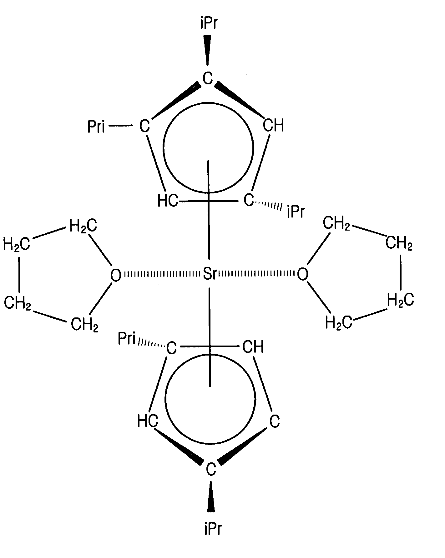
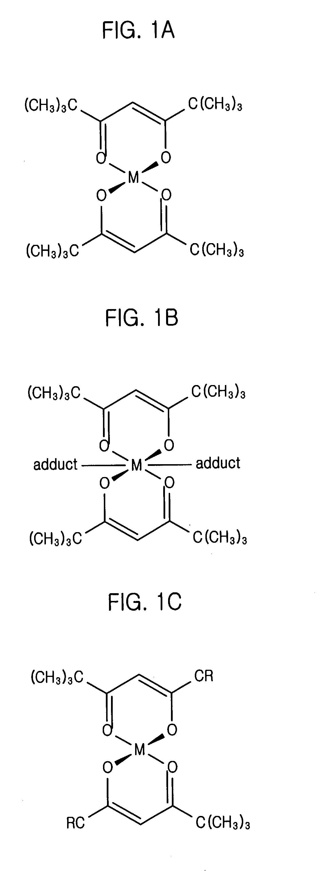
[0025] As a Sr source material, Sr(TMHD).sub.2 is flowed into the reactor the reactor for predetermined time ranging from about 0.1 to about 10.0 seconds, and the Sr source material is absorbed on a surface of a substrate. At this time, a .beta.-diketonate ligand or a cyclopenta ligand combined to a central Sr atom, may be used as the Sr source material. Also, a solution in which the .beta.-diketonate ligand or the cyclopenta ligand combined to a central Sr atom is dissolved in a solvent, such as methanol, tertrahydrofuran (THF) and n-butylacetate, etc., is use...

second embodiment

[0038] the present invention is to form STO layer with ALD method using plasma produced from mixed gas of H.sub.2 and O.sub.2 mixed gas.

[0039] Referring to the second embodiment, a substrate formed a conductive layer for bottom electrode is loaded within a reactor equipping a discharge pump, and then maintaining the substrate to a predetermined temperature ranging from about 100.degree. C. to about 350.degree. C.

[0040] As a Sr source material, Sr(TMHD).sub.2 is flowed into the reactor about predetermined period ranging from about 0.1 to about 10.0 seconds to adsorb the Sr source material on a surface of a substrate. A .beta.-diketonate ligand is combined with a Ba atom, which is a central metal, and the above-mentioned material may be used by dissolving in a solvent, such as methanol, THF and n-butyleacetate, etc.

[0041] To remove a non-react Sr source material, an inert gas, i.e., N.sub.2 and Ar, etc., are flowed into the reactor for a predetermined time ranging from about 0.1 to ab...

third embodiment

[0051] the present invention is form a STO layer with ALD method using plasma, such as N.sub.2O, O.sub.2 and O.sub.3.

[0052] Referring to the first embodiment, a substrate formed a conductive layer for bottom electrode is loaded within a reactor equipping a discharge pump, and then maintaining the substrate to a predetermined temperature ranging from about 200.degree. C. to about 400.degree. C.

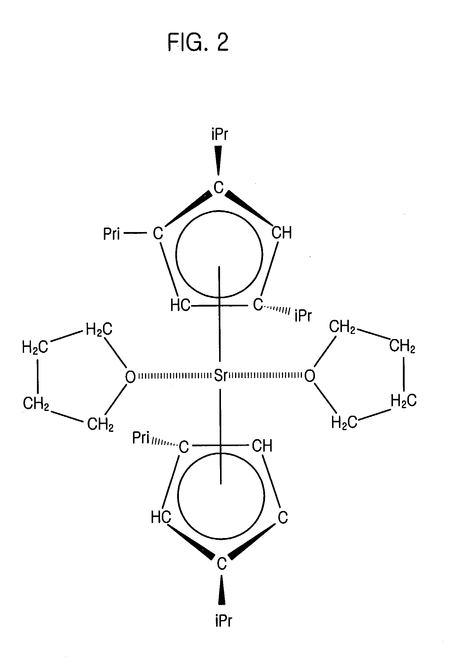
[0053] As a Sr source material, Sr(TMHD).sub.2 is flowed into the reactor about predetermined period ranging from about 0.1 to about 10.0 seconds to adsorb the Sr source material on a surface of a substrate. A .beta.-diketonate ligand uses materials combined with a Sr atom, which is a central metal, or a cyclopenta ligand combined with Sr atom, which is a central metal, may be used and the above-mentioned material may be used by dissolving in a solvent, such as methanol, THF and n-butyleacetate, etc.

[0054] To remove a non-react Sr source material, an inert gas, i.e., N.sub.2 and Ar, etc., are f...


PUM

PropertyMeasurementUnit
temperatureaaaaaaaaaa

Abstract

A method for manufacturing semiconductor device is disclosed which forms a high dielectric layer using atomic layer deposition (ALD). The method for forming a high dielectric layer having a first metal element, a titanium atom and an oxygen atom includes: a) preparing a substrate where a predetermined bottom layer is formed; b) on a surface of the substrate, adsorbing a first organism source combining a ligand, wherein the ligand includes at least oxygen and C-H combination in the first metal element; c) on the surface of the substrate, forming an atomic layer of the first metal element and the oxygen by inducing reduction reaction of the first organism source and a NH3 gas, which are adsorbed on the surface of the substrate; d) on the surface of the substrate where the atomic layer is formed, adsorbing a second organism source combining a ligand, wherein the ligand includes at least oxygen and C-H combination on the titanium; and e) on the surface of the substrate, forming an atomic layer of the titanium and the oxygen by inducing reduction reaction of the second organism source and the NH3 gas, which are adsorbed on the surface of the substrate.

Description

[0001] A method for manufacturing semiconductor device and, more particularly, a method for forming high dielectric layers using an atomic layer deposition (ALD) is disclosed.DESCRIPTION OF THE RELATED ART[0002] With high integration of a semiconductor device, a conventional capacitor based on a Si.sub.3N.sub.4 layer and a SiO.sub.2 layer (so-called, an NO structure) is limited in its ability to acquire a sufficient capacitance per unit area. Accordingly, to obtain a capacitance per unit area, research has been conducted for increasing the surface area of a charge storage electrode. However, because of the reduction of a process margin accompanied with high integration, there exists a limit in increasing surface area of the charge storage electrode.[0003] For overcoming the above-mentioned limit, an interest in a method for manufacturing a high dielectric capacitor, which uses high dielectric materials,-such as SrTiO.sub.3 (hereinafter, referred to STO), BaTiO.sub.3 (hereinafter, re...

Claims


Application Information

Patent Timeline
Patent Type & Authority Applications(United States)
IPC IPC(8): C23C16/40C23C16/44C23C16/00C23C16/455H01L21/316
CPCC23C16/405C23C16/409H01L21/31691C23C16/45542C23C16/45553C23C16/45531H01L21/0228H01L21/02197C23C16/00
Inventor KIL, DEOK-SINJANG, HYUK-KYOO
Owner SK HYNIX INC
Why Eureka
Try Eureka