Encapsulation of organic electronic devices using adsorbent loaded adhesives

a technology of organic electronic devices and adhesives, applied in the direction of discharge tubes luminescnet screens, other domestic articles, etc., can solve the problems of heat, light, oxygen, and moisture adversely affecting many inorganic materials, and achieve the effect of convenient application of adhesive sealants

Inactive Publication Date: 2003-07-31
3M INNOVATIVE PROPERTIES CO
View PDF0 Cites 180 Cited by
  • Summary
  • Abstract
  • Description
  • Claims
  • Application Information

AI Technical Summary

Benefits of technology

0004] The present invention recognizes the need for effective, easy-to-apply adhesive sealants containing adsorbent materials. The present invention features the use of adsorbent (desiccant and/or getterer) loaded transfer adhesives to adhere an encapsulat

Problems solved by technology

Heat, light, oxygen, and moisture adversely affect many of the inorganic materials, s

Method used


Image

  • Encapsulation of organic electronic devices using adsorbent loaded adhesives
  • Encapsulation of organic electronic devices using adsorbent loaded adhesives
  • Encapsulation of organic electronic devices using adsorbent loaded adhesives

Examples


example 1

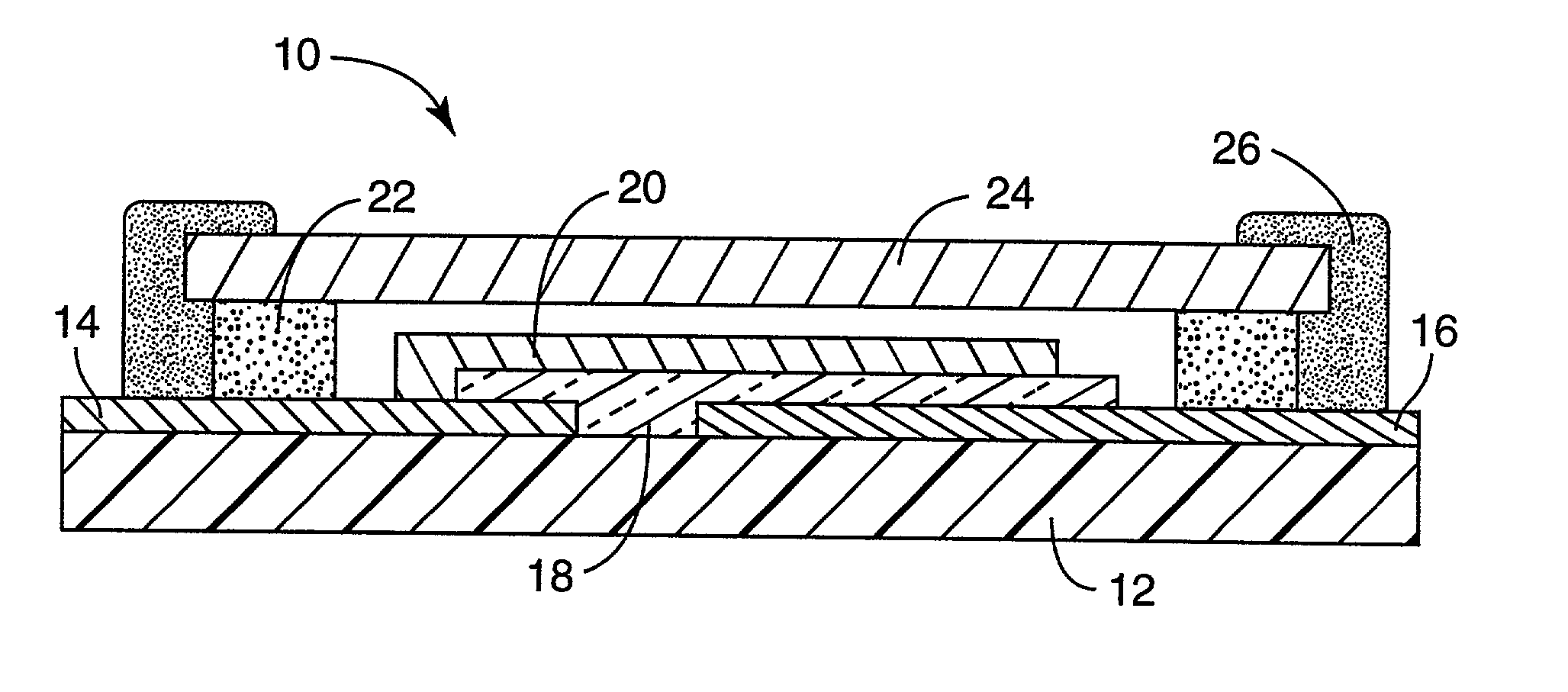
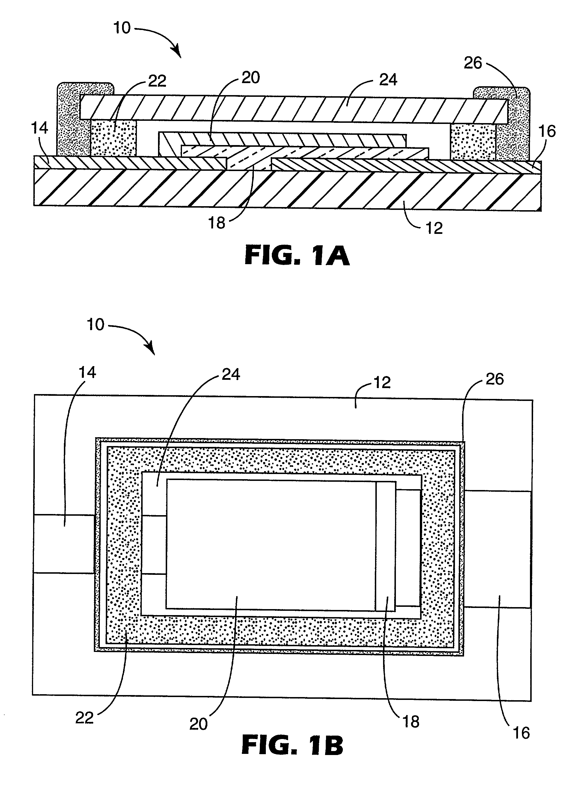
[0043] This example describes the making of an OLED with a gasket-like adsorbent-loaded adhesive layer. FIG. 1 is an illustration of an OLED device made as described in this example.

[0044] A 2".times.3" indium tin oxide (ITO), coated glass slide, available from Thin Film Devices, Long Beach, Calif., was etched to form a simple pattern of two ITO pads (electrodes) with a small (1-3 mm) gap in between. The etching took place in a heated hydrochloric acid bath (about 60.degree. C.) and the masking was accomplished using a commercially available plating tape. Following completion of the etching, the tape was removed and the unetched portion of the ITO on glass was cleaned using a methanol rub and oxygen plasma exposure. A thin film of poly(ethylenedioxythiophene) (PEDOT) (available as product number 4083 from Bayer,Pittsburgh, Pa.) was deposited on the surface by spin coating (not shown in FIG. 1). The PEDOT coated ITO on glass was baked on a hotplate at about 100.degree. C. for about 5...

example 2

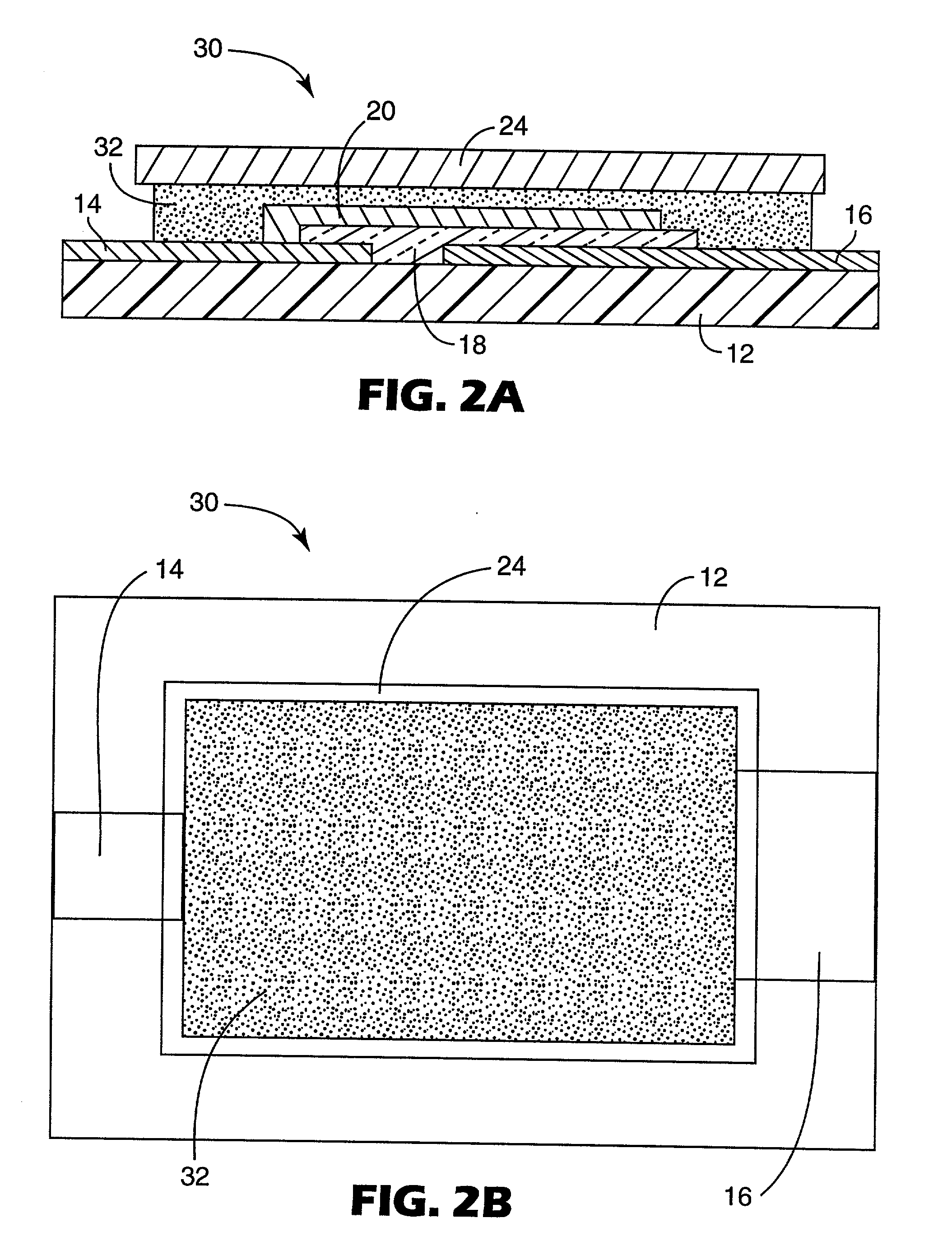
[0049] This example describes the making of an OLED with a continuous adsorbent-loaded adhesive layer. FIG. 2 is an illustration of an OLED device made as described in this example.

[0050] An unencapsulated OLED device was made in the same manner as described in Example 1. Also as in Example 1, upon completion of the thin film stack deposition the sample was removed from the vacuum system and immediately introduced into a nitrogen glove box. A thin (0.2 mm) glass slide was used as the encapsulating lid. It was placed on a hotplate in the nitrogen glove box and heated to about 130.degree. C.

[0051] A rectangular piece of the dessicant loaded hotmelt adhesive film of Example 1 was cut out with scissors to fit directly over (and almost entirely cover) the thin glass encapsulating lid. The resulting adhesive piece was placed on top of the hot encapsulating lid, began to soften and develop a wet appearance after about 3-5 minutes. Following this change, the OLED lamp was placed cathode sid...


PUM

PropertyMeasurementUnit
Fractionaaaaaaaaaa
Fractionaaaaaaaaaa
Flexibilityaaaaaaaaaa

Abstract

Disclosed herein are organic electronic devices that are encapsulated at least in part by adsorbent-loaded transfer adhesives. The adsorbent material may be a dessicant and/or a getterer. The adsorbent-loaded transfer adhesive may form a gasket around the periphery of the device, or may cover the entire device and its periphery. An encapsulating lid covers the device.

Description

TECHNICAL FIELD[0001] This invention relates to encapsulated organic electronic devices.BACKGROUND[0002] Organic electronic devices (OEDs) are articles that include layers of organic materials, at least one of which can conduct an electric current. Illustrative examples of known OED constructions include organic transistors, photovoltaic devices, rectifiers, and organic light emitting diodes (OLEDs). Heat, light, oxygen, and moisture adversely affect many of the inorganic materials, such as low work function electrodes, and the organic materials that are used in OEDs. It is important, therefore, to protect these materials from exposure to the open air. OED devices thus require hermetic packaging in order to achieve the long lifetimes required for many applications. For an OLED, this typically consists of attaching a glass or metal cap onto the cathode side of the device, as described in, e.g., U.S. Pat. Nos. 5,874,804 and 5,686,360, respectively. As described in, e.g., JP 00123968, ...

Claims


Application Information

Patent Timeline
IPC IPC(8): H05B33/04H01L51/50H01L51/52H05B33/10
CPCH01L51/5237Y10S428/917Y10T428/23Y10T428/239Y10T428/2852H10K50/846H10K50/84H10K50/8426H01L2224/8088H10K50/11
Inventor MCCORMICK, FRED B.BAUDE, PAUL F.HAASE, MICHAEL A.
Owner 3M INNOVATIVE PROPERTIES CO
Why Eureka
Try Eureka