

Etching method
a technology of etching and etching plate, which is applied in the direction of decorative surface effects, electrical equipment, decorative arts, etc., can solve the problems of difficult control of the change in percentage, unsuitable wet process for treating wafers of a large diameter, and prone to change in selective ratio, etc., and achieve the effect of shortening the necessary tim
- Summary
- Abstract
- Description
- Claims
- Application Information
AI Technical Summary
Benefits of technology
Problems solved by technology
Method used
Image

Examples
embodiment 1
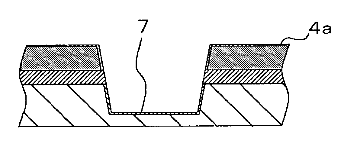
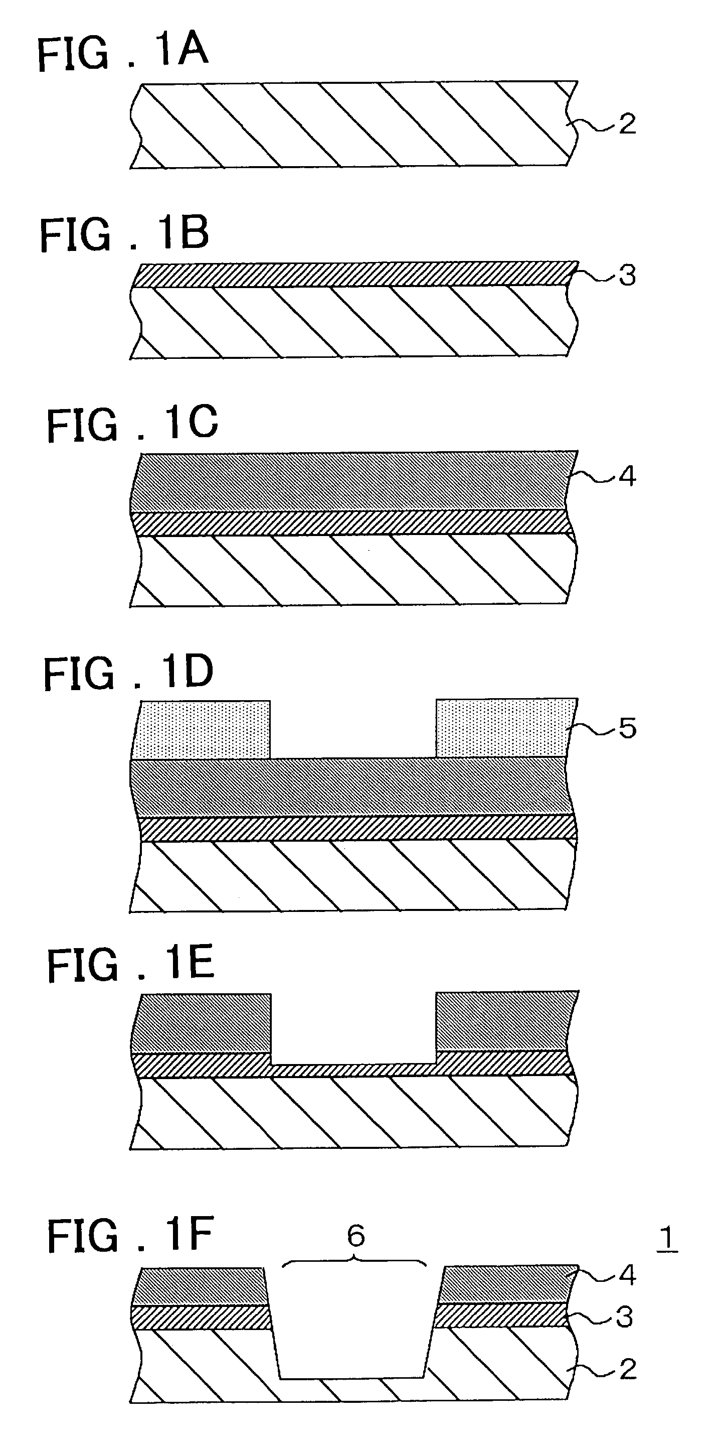
[0039] In the semiconductor substrate (a wafer) used in embodiment 1, a trench 6 is formed in a silicon substrate 2 formed a silicon nitride film 4 and a silicon oxide film 3 as shown in FIG. 1F. The semiconductor substrate 1 is formed by the following steps.
[0040] First, the silicon oxide film 3 of 5-15 nm in film thickness is formed on a surface of the silicon substrate 2 by heat oxidation (Refer to FIG. 1B). Second, the silicon nitride film 4 (LP-Si.sub.3N.sub.4 film) of 100-150 nm in film thickness is formed on the silicon oxide film 3 by a LPCVD method (Refer to FIG. 1C). Third, a resist pattern 5 is formed on the silicon nitride film 4 by a lithography technology (Refer to FIG. 1D). Fourth, the silicon nitride film 4 and a part of the silicon oxide film 3 are removed by dry etching (anisotropic etching) using the resist pattern 5 as an etching mask until the silicon oxide film 3 is exposed. Then, particles and organic materials are removed by chemicals for cleaning such as SPM...
embodiment 2
[0064] The process temperature of the oxidation step in embodiment 2 is at about 250.degree. C. as stated above but also may be in a range of 200-350.degree. C. Shortening of the process time of the oxidation step is not expected in case where the temperature is lower than 200.degree. C. Demerits that the process time is too short to control or that a cooling time is too long are expected in case where the temperature is higher than 350.degree. C.
[0065] Next, embodiment 3 is explained by using a drawing. FIG. 7 is a systematic view showing a structure of an ashing system used in an etching method of embodiment 3 of the present invention.
[0066] A semiconductor substrate (just before an oxidation step) in embodiment 3 is the same as the semiconductor substrate 1 in FIG. 1F. And, an ashing system 30 used in embodiment 3 comprises a susceptor 34 heated to a constant temperature of about 250.degree. C. instead of the susceptor of the ashing system in FIG. 4, a lift 36, which lift up the ...
embodiment 5
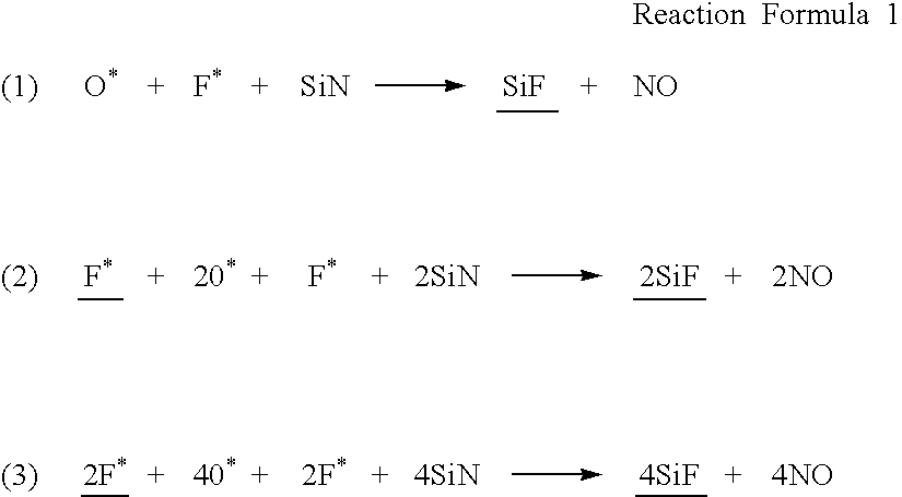
[0072] , it is possible to adjust to increase a quantity of the pullback (a trench opening between patterns of the silicon nitride film). For example, it is possible to etch a quantity of the pullback of about 210 .ANG. (21 nm) (=70 .ANG..times.3 times) in case where the oxidation step and the pullback step, in which the quantity of the pullback per one time is 70 .ANG. (7 nm), are repeated three times. It is unnecessary to use a variant etching system or a chamber (a reaction room) at every step because the oxidation step and the pullback step allow repeating by a process sequence of the etching system.
[0073] Next, embodiment 6 is explained. In an etching method of embodiment 6, each process time of the oxidation step and the pullback step in embodiment 1 is relatively shortened. A semiconductor substrate is the same as the semiconductor substrate 1 in FIG. 1F. An ashing system in embodiment 6 is the same as the ashing system 10 in FIG. 4. According to embodiment 6, it is possible ...
PUM
| Property | Measurement | Unit |
|---|---|---|
| Fraction | aaaaa | aaaaa |
| Pressure | aaaaa | aaaaa |
| Pressure | aaaaa | aaaaa |
Abstract
Description
Claims
Application Information