Semiconductor memory device with internal data reading timing set precisely

a memory device and timing technology, applied in semiconductor devices, digital storage, instruments, etc., can solve the problems of inability to detect accurate timing, disadvantageous optimization of the activation timing of the sense amplifier, and unnecessarily increasing the read cycle tim

Inactive Publication Date: 2003-10-30
RENESAS ELECTRONICS CORP
View PDF3 Cites 25 Cited by
  • Summary
  • Abstract
  • Description
  • Claims
  • Application Information

AI Technical Summary

Problems solved by technology

However, if the word line drive pulse has an extra margin, a read cycle time unnecessarily increases.
Therefore, it becomes disadvantageously difficult to optimize the activation timing of the sense amplifier, activation timing of the bit line precharging and deactivation timing of a selected word line.
Accordingly, if one dummy cell is fixedly selected as disclosed in the foregoing prior art, accurate timing cannot be detected due to variations in transistor characteristics of the selected normal memory cell and the dummy cell.
For example, if the transistor characteristics of the dummy cell may varies to a better characteristics to change the dummy bit line at higher speed, while transistor characteristics of a selected normal memory cell varies to a worse direction to slow down the change of the normal bit line, the deactivation of the word line and the activation of the sense amplifier are performed at excessively early timing so that a malfunction may occur.
For these reasons, it is impossible to achieve the object of reducing the margin in the word line drive timing, and accordingly it becomes impossible to increase an operation speed and to reduce power consumption.
In particular, for various bit / word configurations required in system LSIs and others, the optimum timing values must be set for each configuration, leading to a problem that an extremely long period is required for the design and development.
However, the voltages of these complementary dummy bit lines DBLB0 and DBLB1 are at the precharged voltage level, and are not used for controlling an internal operation.
Therefore, when row decoder 23 transmits the word line select signal to the selected word line, this interconnection resistance causes a delay in signal transmission on the selected word line.
However, this causes no practical problem because dummy bit line DBLB is not used for the voltage detection.
The word line has an interconnection resistance, and causes a delay in signal propagation.
As miniaturization of elements progresses, it becomes difficult to control the pattern final feature sizes in a patterning process due to irregular reflection of exposure light at a stepped portion as well as influences by neighboring layout patterns.
However, it is difficult to effect such correction on a boundary between the extremely miniaturized pattern such as the memory cells and its peripheral pattern because these patterns are quite different in regularity.

Method used


Image

  • Semiconductor memory device with internal data reading timing set precisely
  • Semiconductor memory device with internal data reading timing set precisely
  • Semiconductor memory device with internal data reading timing set precisely

Examples


Embodiment Construction

]

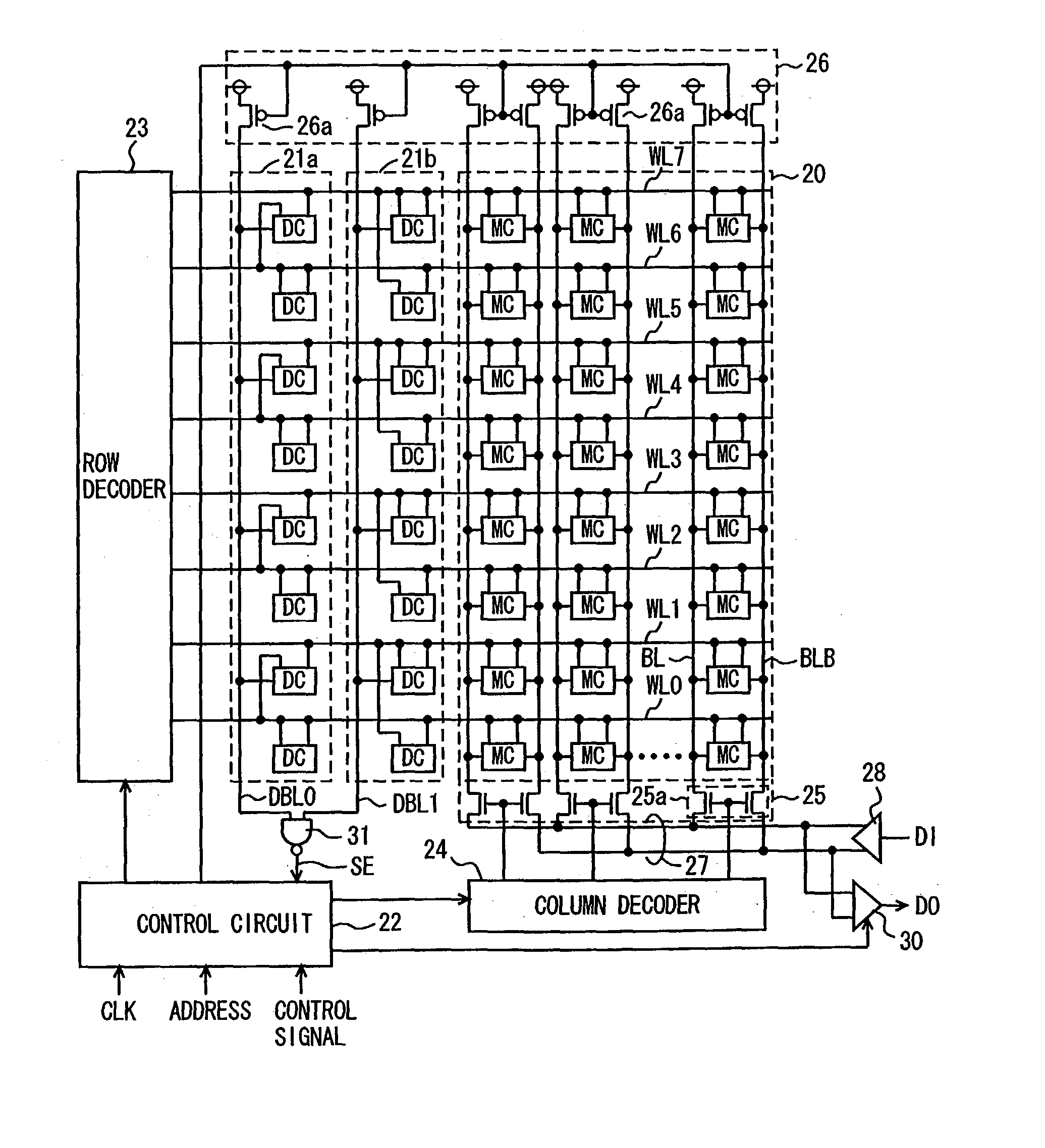
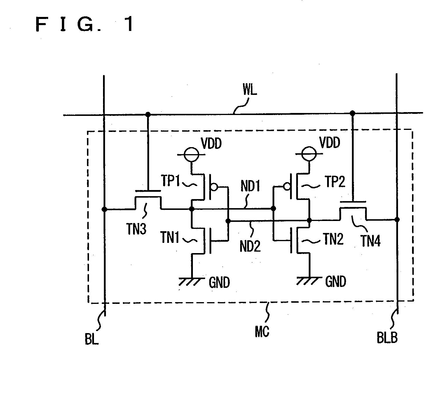
[0286] In the embodiments described above, SRAM is used as the semiconductor memory device. However, for a non-volatile semiconductor memory device such as a flash memory, in which a current flowing a bit line is detected to read data, activation timing of sense amplifier can be internally set accurately using the dummy bit lines as described above. In the case of such a non-volatile semiconductor memory device, the dummy cell is formed of a non-volatile memory cell having the same structure as a normal nonvolatile memory cell for storing data. A word line is formed of a metal interconnection, a control gate of the nonvolatile memory cell is formed of polycrystalline silicon, and a connection between the metal interconnection of the word line and the polycrystalline silicon control gate in the dummy cell is made different from that in the normal memory cell.

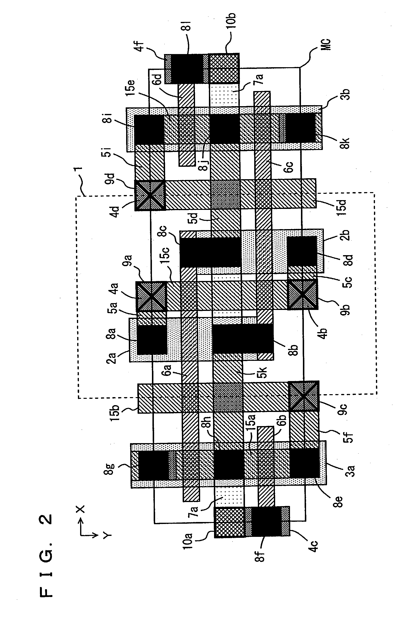
[0287] According to the invention, as described above, the dummy cells are aligned in the row direction with the normal memory...


PUM


Abstract

Dummy cells each having the same layout as a normal memory cell are aligned in a row direction to the normal memory cells, and are arranged in rows and columns. In each dummy cell column, a dummy bit line is arranged, and a plurality of dummy cells are simultaneously selected and connected to the corresponding dummy bit line when one word line is selected. A voltage detecting circuit detects the potentials on the dummy bit lines to determine timing of activation of a sense amplifier. In the semiconductor memory device, the potential on the dummy bit line can be changed at high speed, and internal data read timing can be optimized independent of a structure of a memory cell array.

Description

[0001] 1. Field of the Invention[0002] The present invention relates to a semiconductor memory device, and particularly to a semiconductor memory device, which can internally produce data read timing with accuracy.[0003] 2. Description of the Background Art[0004] In a static RAM (Random Access Memory), a word line drive pulse having a predetermined active period is produced in accordance with a change in address signal, and is applied to a word line. This word line drive pulse is produced with a sufficient margin in advance, so that correct data can be reliably read out even if a time required for data reading changes due to variations in process, change in ambient temperature and other(s). However, if the word line drive pulse has an extra margin, a read cycle time unnecessarily increases.[0005] Japanese Patent Laying-Open No. 11-339476, for example, discloses a method, in which a read signal read from a dummy memory cell is supplied to a word line drive circuit or a row decoder fo...

Claims


Application Information

Patent Timeline
Patent Type & Authority Applications(United States)
IPC IPC(8): G11C11/419G11C7/22G11C11/41H01L21/8244H01L27/11
CPCG11C7/22G11C7/227G11C2207/2281G11C29/24G11C29/023G11C29/026G11C29/028G11C2207/229G11C29/00
Inventor NII, KOJINAKASE, YASUNOBU
Owner RENESAS ELECTRONICS CORP
Why Eureka
Try Eureka