Gold-silver bonding wire for semiconductor device

a technology of silver-silver bonding and semiconductor devices, which is applied in the direction of solid-state devices, semiconductor devices, basic electric elements, etc., can solve the problems of gold being highly ductile and malleable, the breakage occurring near the ball neck in the loop formation remains unsolved, and the reliability is low

Inactive Publication Date: 2003-11-13
MK ELECTRON
View PDF0 Cites 25 Cited by
  • Summary
  • Abstract
  • Description
  • Claims
  • Application Information

AI Technical Summary

Problems solved by technology

In addition, the problem of the breakage occurring near the ball neck in the loop formation remains unsolved.
Furthermore, the ball grain refinement in Japanese Laid-open Patent Application No. 2000-150562 increases the area of grain boundaries acting as Au and Ag atom diffusion paths, and thus it is likely to lower reliability.
Also, gold is highly ductile and malleable.
However, gold is greatly affected by peripheral temperature variations and tends to expand at a high temperature.
In addition, because the mechanical strength of gold is weak, when a gold bonding wire is applied to interconnects in a semiconductor package, wire loops forming the interconnects may sag or sweep.
As a result, a reduction in thermal reliability is prevented.
According to the results of a variety of experiments, when the elements of the first group are added in an amount of less than 50 ppm by weight, there is no effect of improving thermal reliability.
When the elements of the first group are added in an amount of greater than 10,000 ppm by weight, ball hardness is increased and chip cracks occur.
When the elements of the second group are added in an amount of greater than 50 ppm by weight, it is difficult to form a whole spherical free air ball due to dimple formation.
When the elements of the third group are added in an amount of greater than 50 ppm by weight, the tensile strength is reduced, and thus it is likely to occur a brittle failure near the ball neck.

Method used


Image

  • Gold-silver bonding wire for semiconductor device
  • Gold-silver bonding wire for semiconductor device

Examples


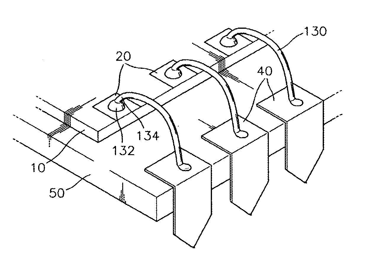
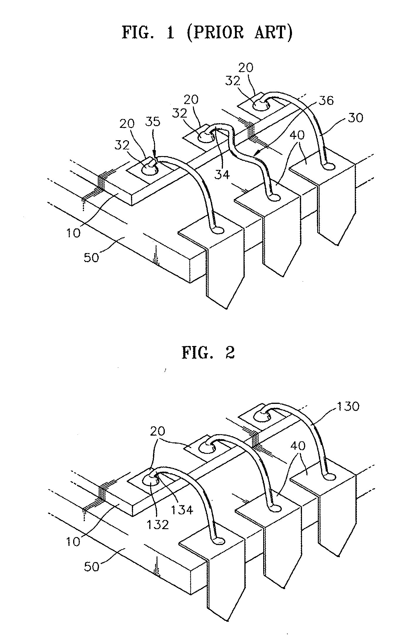
Embodiment Construction

53 0.1 20 5 10 36 4 20 37 15 0.03 38 45 1 0.002 39 30 1 150 40 10 1 5 20

[0034] With the bonding wires prepared in the compositions of Table 1, the following experimental results in Table 2 were obtained. As shown in Table 2, tensile strength as a mechanical characteristic of the bonding wires, degree of loop sweeping, bondability after bonding and after a thermal process, loop height deviation, loop shape, ball shape, and ball hardness were measured.

[0035] The tensile strength was measured with respect to breaking load and elongation using an AND RTC 1150A instrument at a cross head speed of 10 mm / min and a gage length of 100 mm at 20.degree. C.

[0036] The degree of loop sweeping was measured by molding the bonded chip and lead frame with an epoxy molding compound resin and imaging the same using transmission X-rays. A loop displacement in the direction in which the epoxy molding compound resin flows was measured, and a percentage of the loop displacement with respect to the distance...


PUM

PropertyMeasurementUnit
speedaaaaaaaaaa
purityaaaaaaaaaa
weightaaaaaaaaaa

Abstract

A gold-silver alloy bonding wire for a semiconductor device is provided. The bonding wire contains: a Au-Ag alloy including 5-40% Ag by weight in Au having a purity of 99.999% or greater; at least one element of a first group consisting of Pd, Rh, Pt, and Ir in an amount of about 50-10,000 ppm by weight; at least one element of a second group consisting of B, Be, and Ca in an amount of about 1-50 ppm by weight; at least one element of a third group consisting of P, Sb, and Bi in an amount-of about 1-50 ppm by weight; and at least one element of a fourth group consisting of Mg, TI, Zn, and Sn in an amount of about 5-50 ppm by weight. The bonding wire is highly reliable with a strong tensile strength at room temperature and high temperature and favourable bondability. When the bonding wire is looped, no rupture occurs in a ball neck region. Also, no chip cracking occurs since the ball is soft.

Description

[0001] 1. Field of the Invention[0002] The present invention relates to a bonding wire for electrically connecting a semiconductor chip and a lead frame or a printed circuit board (PCB) in a packaging process, and more particularly, to a bonding wire which does not cause chip cracks because it forms a soft ball.[0003] 2. Description of the Related Art[0004] Referring to FIG. 1, a general semiconductor package includes a semiconductor chip 10 on a pad 50, a plurality of chip pads 20 formed on the semiconductor chip 10 as input / output ports for a variety of signals, a plurality of lead frames 40 electrically connected to the semiconductor chip 10 to receive the variety of signals from or to output the same to an external circuit; and a bonding wire 30 for electrically connecting the chip pad 20 and the lead frame 40. This structure of the general semiconductor package is protected by, for example, epoxy molding compound resin.[0005] One end of the bonding wire 30 bound to the chip pad...

Claims


Application Information

Patent Timeline
Patent Type & Authority Applications(United States)
IPC IPC(8): H01L21/60H01L23/49
CPCH01L24/45H01L2224/48624H01L2224/45015H01L2224/45144H01L2224/48091H01L2224/48247H01L2224/48465H01L2924/01004H01L2924/01005H01L2924/01006H01L2924/01012H01L2924/01013H01L2924/01015H01L2924/0102H01L2924/01022H01L2924/01029H01L2924/0103H01L2924/01046H01L2924/01047H01L2924/01049H01L2924/0105H01L2924/01051H01L2924/01057H01L2924/01077H01L2924/01078H01L2924/01079H01L2924/01082H01L2924/01083H01L2924/01205H01L2924/01327H01L2924/20752H01L2224/05624H01L2924/01045H01L2924/01033H01L2924/00014H01L2924/00011H01L2924/01081H01L2924/00H01L2924/013H01L24/43H01L2924/181H01L2224/43H01L2224/05554H01L21/60
Inventor MOON, JEONG-TAKCHO, JONG-SOOJOUNG, DONG-HO
Owner MK ELECTRON
Why Eureka
Try Eureka